Light-emitting diode with prevention of electrostatic damage

a technology of light-emitting diodes and electrostatic damage, which is applied in the direction of diodes, semiconductor devices, semiconductor/solid-state device details, etc., can solve the problems of increasing manufacturing difficulty correspondingly, damage, and wasting costs, and achieves the effect of simplifying the manufacturing process and reducing manufacturing costs

Inactive Publication Date: 2005-07-21
OPTO TECH
View PDF1 Cites 35 Cited by
  • Summary
  • Abstract
  • Description
  • Claims
  • Application Information

AI Technical Summary

Benefits of technology

[0007] For this purpose, how to design a novel light-emitting diode (LED) device which, aiming at disadvantages of above conventional art, may not only prevent the LED from being damaged by electrostatic discharge, but also simplify the manufacturing process and reduce the manufacturing cost, is the key point of the present invention.

Problems solved by technology

Whether in the manufacturing process or in use, it is common for the LED to be damaged owing to an electrostatic discharge effect.
Although the function of preventing the LED 10 from being damaged by electrostatic discharge is provided in the above conventional LED device, this LED 10 must be inverted and then fixed on the zener diode 20 in a manufacturing process, which requires a precision alignment equipment, thus not only expending cost, but also increasing manufacturing difficulty correspondingly.
Moreover, with this design, in which the zener diode 20 is used as a sub mount of the LED 10, a great deal of material and manufacturing cost may be wasted owing to the considerable bulkness of this zener diode 20.

Method used


Image

  • Light-emitting diode with prevention of electrostatic damage
  • Light-emitting diode with prevention of electrostatic damage
  • Light-emitting diode with prevention of electrostatic damage

Examples


Embodiment Construction

[0021] The structural features and the effects to be achieved may further be understood and appreciated by reference to the presently preferred embodiments together with the detailed description.

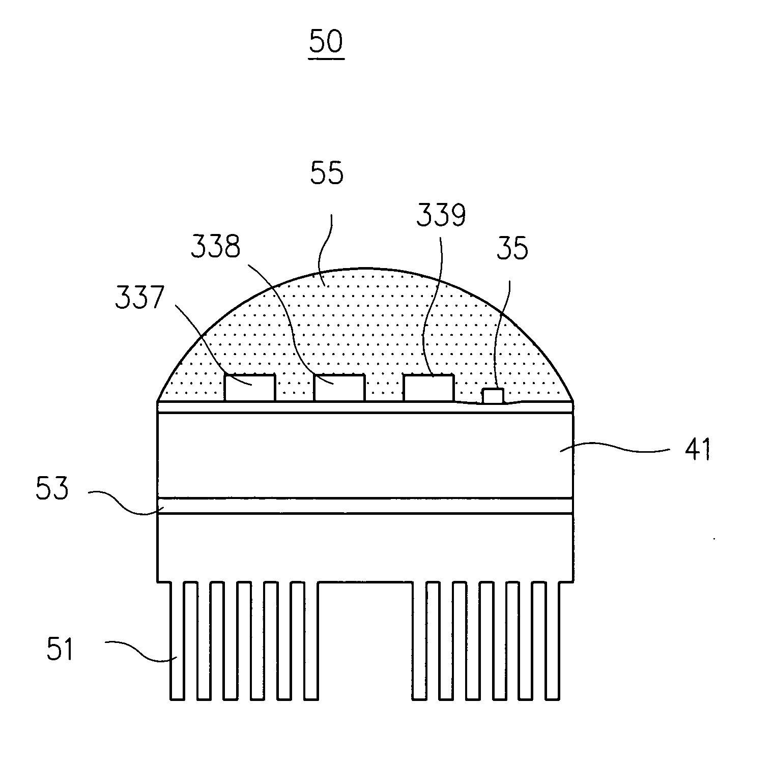
[0022] Referring to FIGS. 3A and 3B, firstly, there are shown a structural exploded diagram according to one preferred embodiment of the present invention and an assembled diagram thereof, respectively. A light-emitting diode (LED) device 30 with prevention of electrostatic damage of the present invention is formed mainly by inverting a LED 33 and an electrostatic discharge protection device 35 in the manner of flip chip, followed by adhering them having being inverted in the manner of flip chip onto a surface insulated substrate 31 having at least one first power supply circuit 311 and at least one second power supply circuit 313.

[0023] In this case, the LED 33, such as a flat LED illustrated in this embodiment, may comprise a LED second electrode 333 and a LED first electrode 331; while ...


PUM


Abstract

A light-emitting diode (LED) device with prevention of electrostatic damage, mainly comprises a surface insulated substrate onto which at least one power supply circuit and at least one second power supply circuit are provided, the former being electrically connected to a LED first electrode of a LED and a ESD second electrode of an electrostatic discharge protection device, while the latter being electrically connected to a LED second electrode of the LED and a ESD first electrode of the electrostatic discharge protection device, in such a way that an inverse-parallel circuit is formed by the LED and the electrostatic discharge protection device. Thus, not only a simplified manufacturing process and raised yield rate, but also a prolonged service life of the LED device may be obtained, due to the feature that active areas of the first power supply circuit and second power supply circuit are larger than those of the ESD first electrode and ESD second electrode.

Description

FIELD OF THE INVENTION [0001] The present invention is related to a light-emitting diode device, particularly to a light-emitting diode device with prevention of electrostatic damage, facilitating not only a simplified manufacturing process and raised yield rate, but also a prolonged service life of the light-emitting diode device. BACKGROUND [0002] Light-emitting diodes (LEDs) have been widely used in computer peripherals, communication products, and other electronic equipments owing to advantages, such as small volume, light weight, lower power consumption, and long service life, as examples. Whether in the manufacturing process or in use, it is common for the LED to be damaged owing to an electrostatic discharge effect. Therefore, how to avoid misgivings about the damage to the LED resulted from this electrostatic discharge effect is the major key point in the design and manufacture of the LED device. [0003] Referring FIG. 1, there is shown a circuit diagram of a conventional LED...

Claims


Application Information

Patent Timeline
Patent Type & Authority Applications(United States)
IPC IPC(8): H01L33/00H01L23/60H01L25/075H01L25/16H01L27/02H01L29/22
CPCH01L25/0753H01L25/167H01L27/0255H01L2224/73265H01L2224/48091H01L2924/12032H01L2924/01322H01L2924/00H01L2924/00014
Inventor LIN, MING-DERLIN, SAN BAO
Owner OPTO TECH
Why Eureka
Try Eureka