

Method for forming a polycide gate and structure of the same
- Summary
- Abstract
- Description
- Claims
- Application Information
AI Technical Summary
Problems solved by technology
Method used
Image

Examples
Embodiment Construction
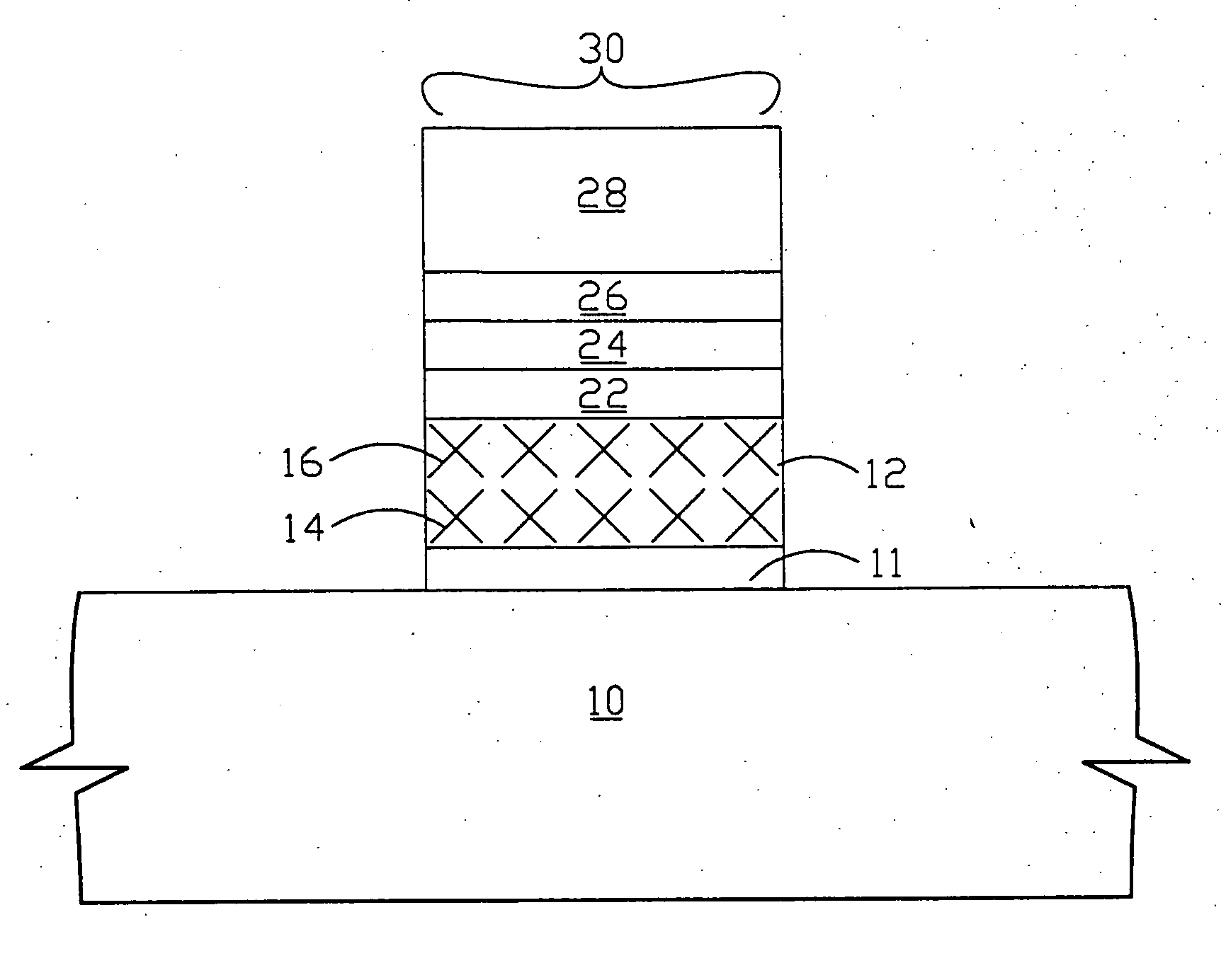
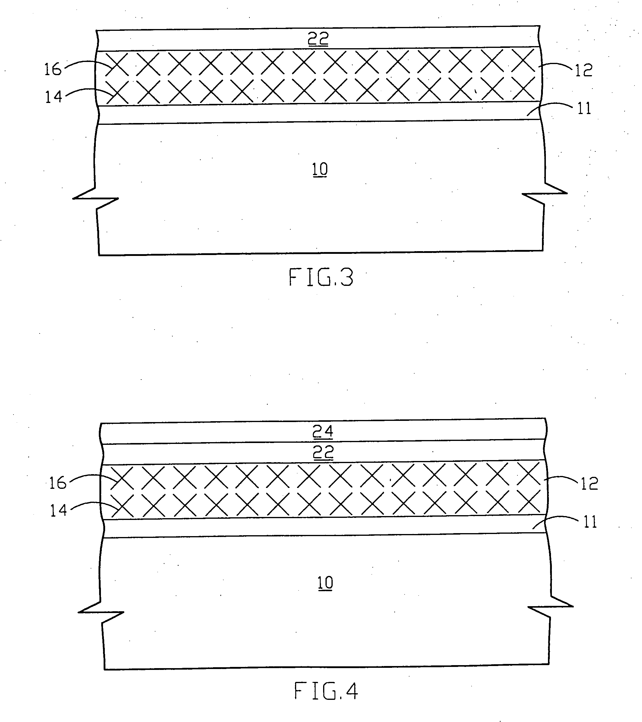
[0024] The present invention proposes a novel method to fabricate the polycide gate and the structure of the same. The aspect of the present invention includes that the polycide gate has a double implantation region of polysilicon. The detail description of the method will be seen as follows.
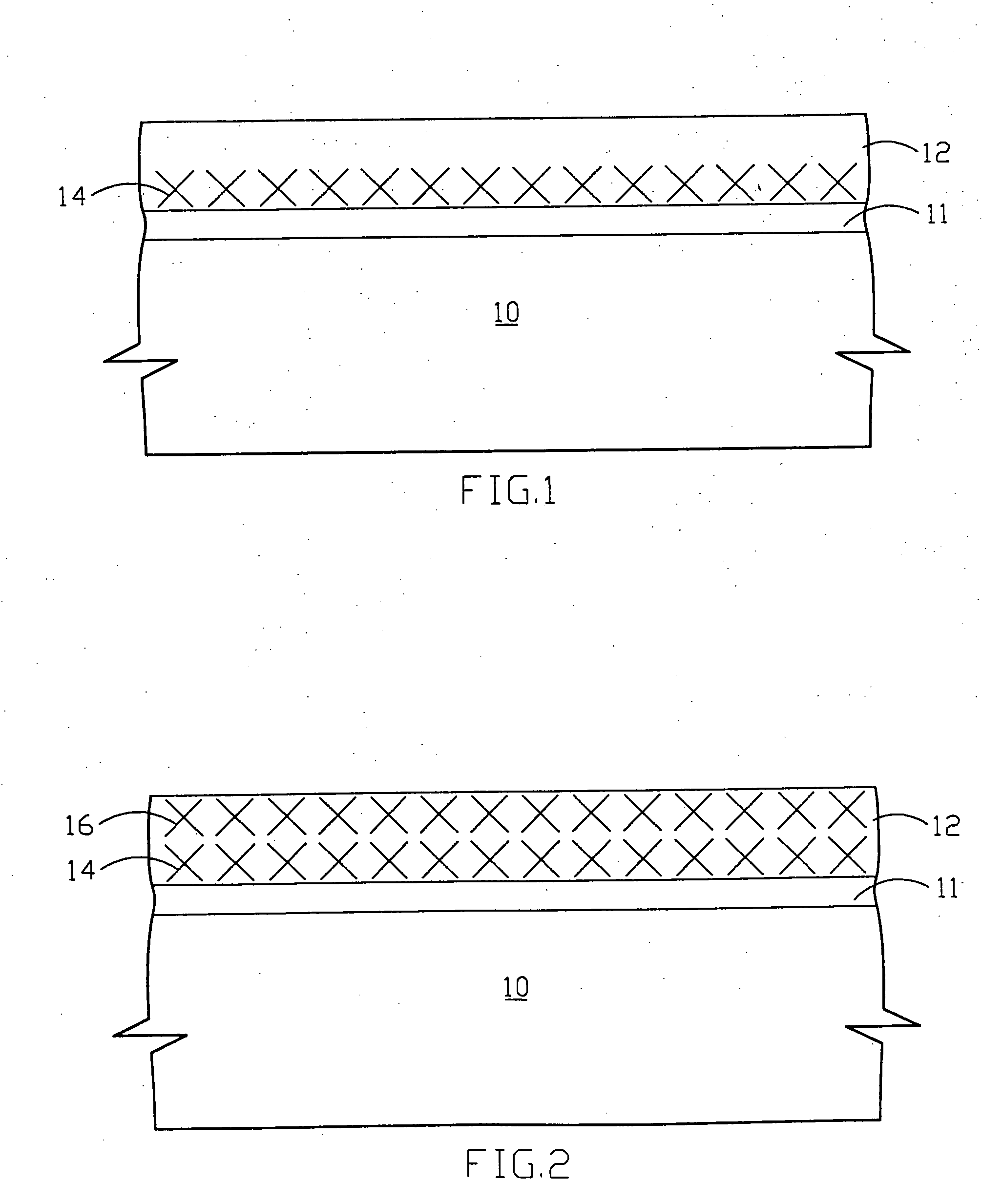
[0025] Turning to FIG. 1, it shows the cross sectional view of forming a deep implantation region of polysilicon according to the present invention. The first procedure of the present invention is to form the silicon dioxide layer 11 on a substrate 10.
[0026] The substrate 10 for forming a gate of semiconductor device according to the present invention suitably includes a single crystal wafer 10 with a or crystallographic orientation. Other substrate material may be used. In a preferred embodiment, a silicon dioxide layer 11 is formed to a thickness of about 10 to 100 angstroms. However, the silicon dioxide layer 11 is suitably formed using thermal oxidation method. The temperature for this p...
PUM
 Abstract
Description
Claims
Application Information