

Semiconductor device and manufacturing method thereof
a technology of semiconductor devices and manufacturing methods, applied in semiconductor devices, semiconductor/solid-state device details, electrical apparatus, etc., can solve the problems of insufficient laser energy fuse cannot be disconnected, etc., to achieve the effect of reducing the proportion of fuse disconnection fault and erroneous disconnection of fuse, facilitating film thickness control over the film above the fuse and facilitating the production of semiconductor devices
- Summary
- Abstract
- Description
- Claims
- Application Information
AI Technical Summary
Benefits of technology
Problems solved by technology
Method used
Image

Examples
second embodiment
[0084] In this embodiment, a guard ring is provided for a layer underlying a region in which the fuse 122 (or fuses) is (are) formed in a configuration shown in the first embodiment so as to prevent entry of moisture after disconnection of the fuse.
[0085] A configuration of this embodiment will be described. Incidentally, same reference characters are assigned to the same configurations as in the first embodiment, and their detailed description will be omitted.
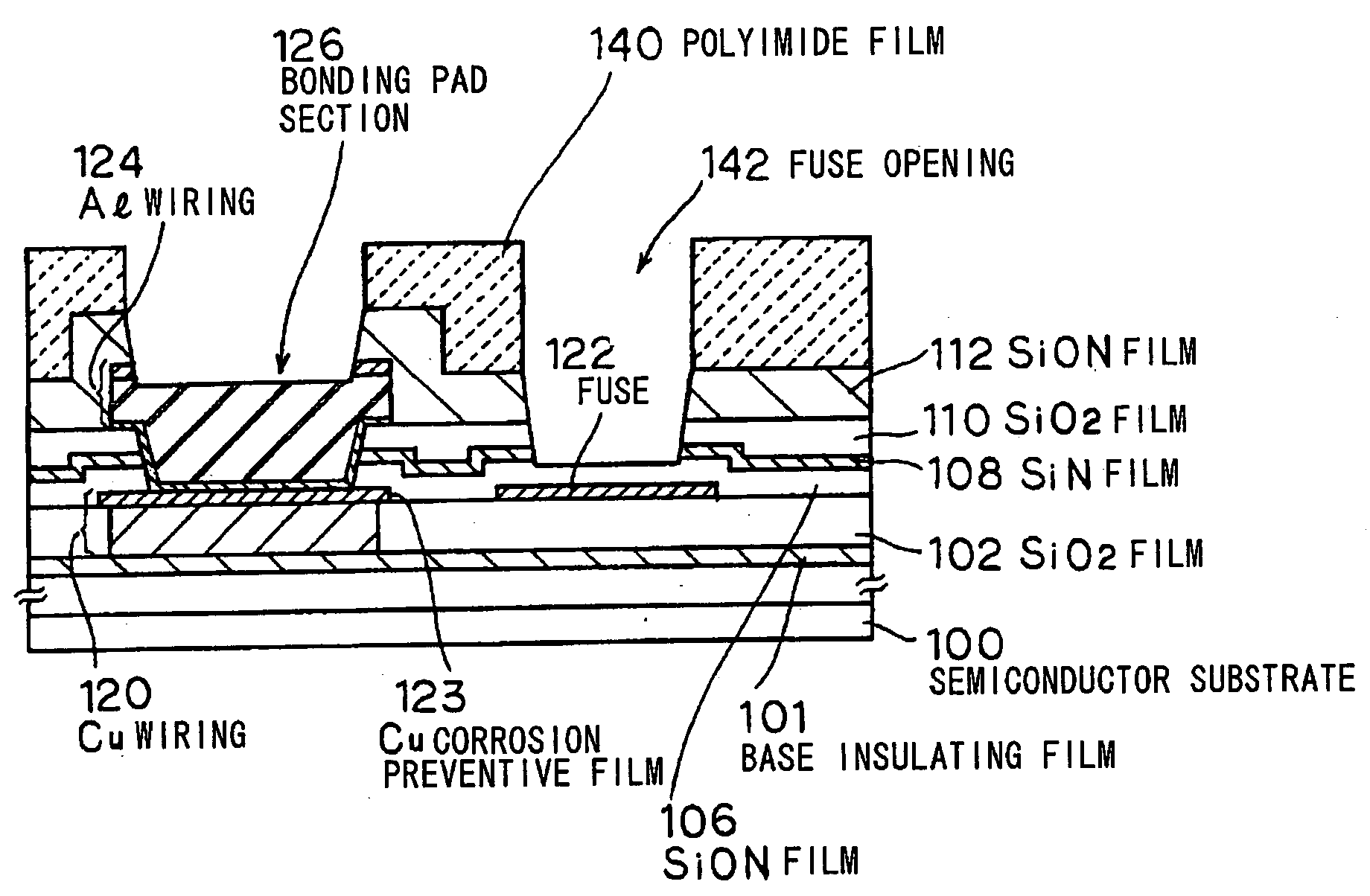
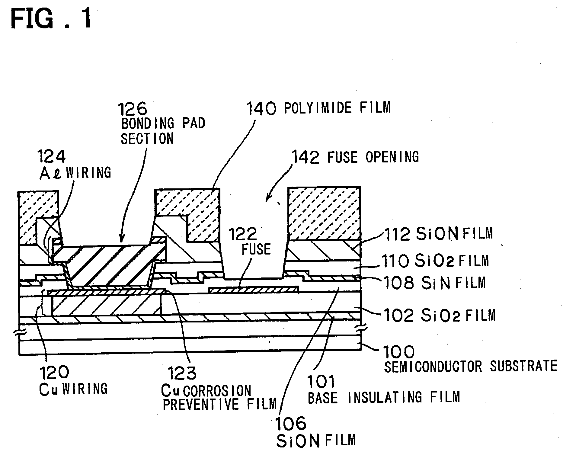
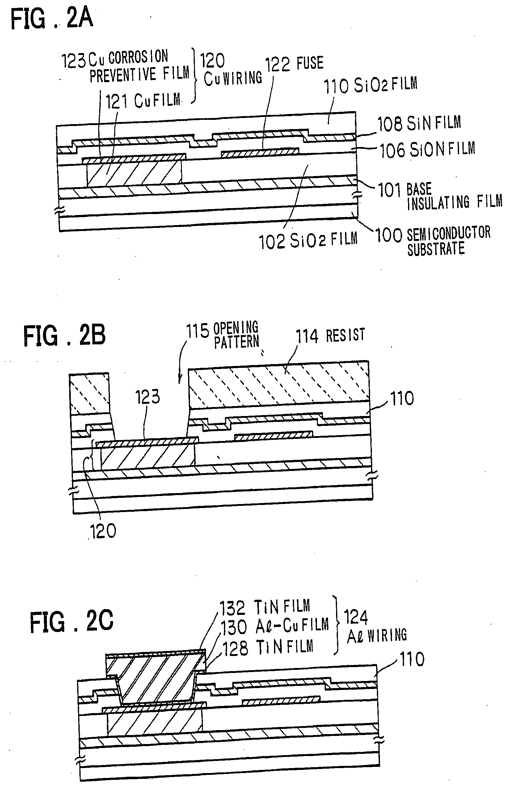
[0086]FIG. 4A is a schematic sectional view showing an example of the configuration of this embodiment. FIG. 4B is a schematic plan view showing layer patterns of the Cu wiring 120 and the fuses 122, and a sectional view along a line section X-X′ corresponds to FIG. 4A.
[0087] As shown in FIGS. 4A and 4B, a guard ring 150 surrounding the planar pattern region of the fuses 122 is formed in the SiO2 film 102 underlying the fuses 122, using the Cu wiring. More specifically, the guard ring 150 is formed, being embedded in the Si...
PUM
 Abstract
Description
Claims
Application Information