

Optical waveguide and method of manufacturing the same
- Summary
- Abstract
- Description
- Claims
- Application Information
AI Technical Summary
Benefits of technology
Problems solved by technology
Method used
Image

Examples
second example
(2) SECOND EXAMPLE
[0096] As the sample, like the first example, the silicon oxide film was formed on the substrate subject to film-forming. This silicon oxide film was formed under following film forming conditions by the plasma CVD method.
[0097] (Film Forming Conditions II)
[0098] (i) Film Forming Gas Conditions
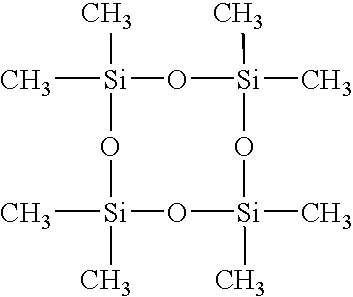
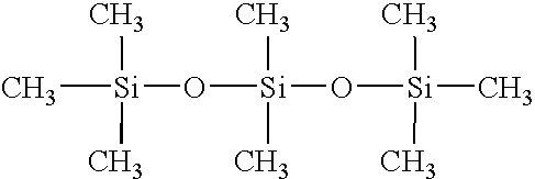
[0099] tetramethylsilane flow rate: 50 sccm
[0100] N.sub.2O flow rate: 2000 sccm
[0101] gas pressure: 1.0 Torr
[0102] (ii) Plasmanizing Conditions
[0103] high-frequency power (13.56 MHz) PRF: 150 W
[0104] low-frequency power (380 kHz) PLF: 300 W
[0105] (iii) Substrate heating temperature: 300.degree. C.
[0106] (iv) Silicon oxide film formed (see FIG. 4)
[0107] film thickness (in-plane): 3.00326 .mu.m.+-.30 nm
[0108] refractive index (in-plane): 1.4642+0.0006
[0109] (measure wavelength: 1.55 .mu.m)
[0110] As described above, according to the above experiment, the silicon oxide film having the small refractive index of about 1.4 could be formed by using the above gas mixture, and also the...
PUM
 Abstract
Description
Claims
Application Information