Thin-film magnetic head and method of forming the same

a magnetic head and thin film technology, applied in nanoinformatics, instruments, record information storage, etc., can solve the problems of alumina surface roughness, alumina thickness is typically corroded and rough, and it is difficult to control the thickness of the lower shielding layer. , to achieve the effect of easy control of the thickness of the film, high accuracy

Inactive Publication Date: 2005-02-17
TDK CORPARATION
View PDF15 Cites 1 Cited by
  • Summary
  • Abstract
  • Description
  • Claims
  • Application Information

AI Technical Summary

Benefits of technology

[0008] Taking into account the above-mentioned problems with the conventional process of forming a partial lower shielding layer, it is an object of the present invention to provide a thin-film magnetic head and a method of forming the thin-film magnetic head, which can easily control a film thickness of the lower shielding layer with no need for additional formation on an alumina film. Also, it is an object of the present invention to provide a thin-film magnetic head and a method of forming the thin-film magnetic head, which can define a track width of a magnetoresistive sensor with high accuracy, the sensor being formed after forming the lower shielding layer, and which is adaptable for a tendency toward a narrower track.

Problems solved by technology

The above-described conventional method of forming the partial lower shielding layer, however, essentially requires expensive equipment and an additional step for forming analumina film.
However, because polishing rates of alumina and a soft magnetic material, such as Permalloy, are substantially equal to each other, it is typically difficult to control the film thickness of the lower shielding layer (i.e., deciding when to end the CMP step).
Further, the alumina surface is typically corroded and roughed with the use of a strong-acid slurry.
In addition, in a photolithography step of forming a resist layer to define a track width of a magnetoresistive sensor, a film thickness distribution of the resist layer is not uniform and a variation may occur in the track width of the magnetoresistive sensor.

Method used


Image

  • Thin-film magnetic head and method of forming the same
  • Thin-film magnetic head and method of forming the same
  • Thin-film magnetic head and method of forming the same

Examples


Embodiment Construction

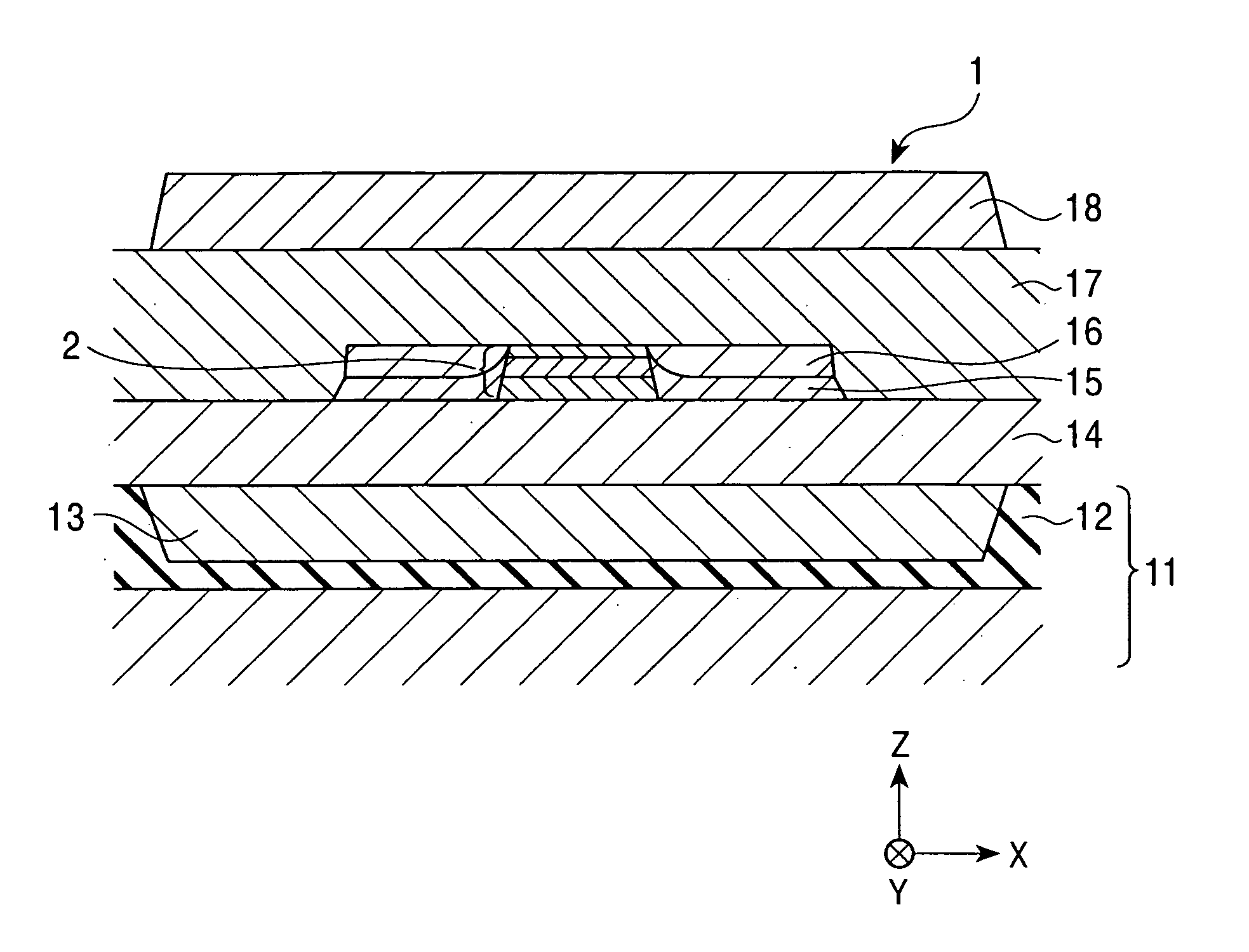
[0026]FIG. 1 is a sectional view, as viewed from the side of a head surface (ABS surface) positioned to face a recording medium, showing an overall multilayered structure of a thin-film magnetic head 1 according to a first embodiment of the present invention. The thin-film magnetic head 1 is a thin-film magnetic head for reproduction, which is provided at a trailing-side end of a floating slider of a hard disk drive, for example. In FIG. 1, X-, Y- and Z-directions are defined respectively as a direction of a track width, a direction of a magnetic field leaked from the recording medium, and a moving direction of the recording medium.

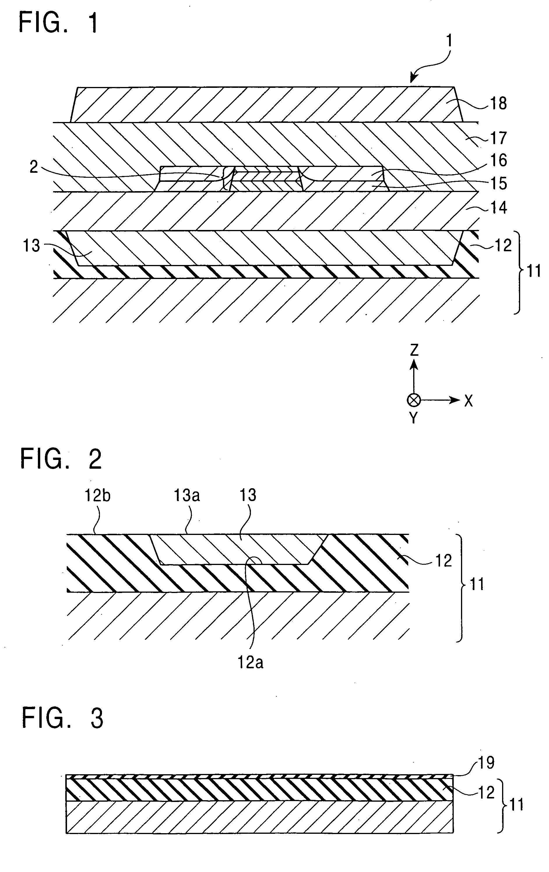
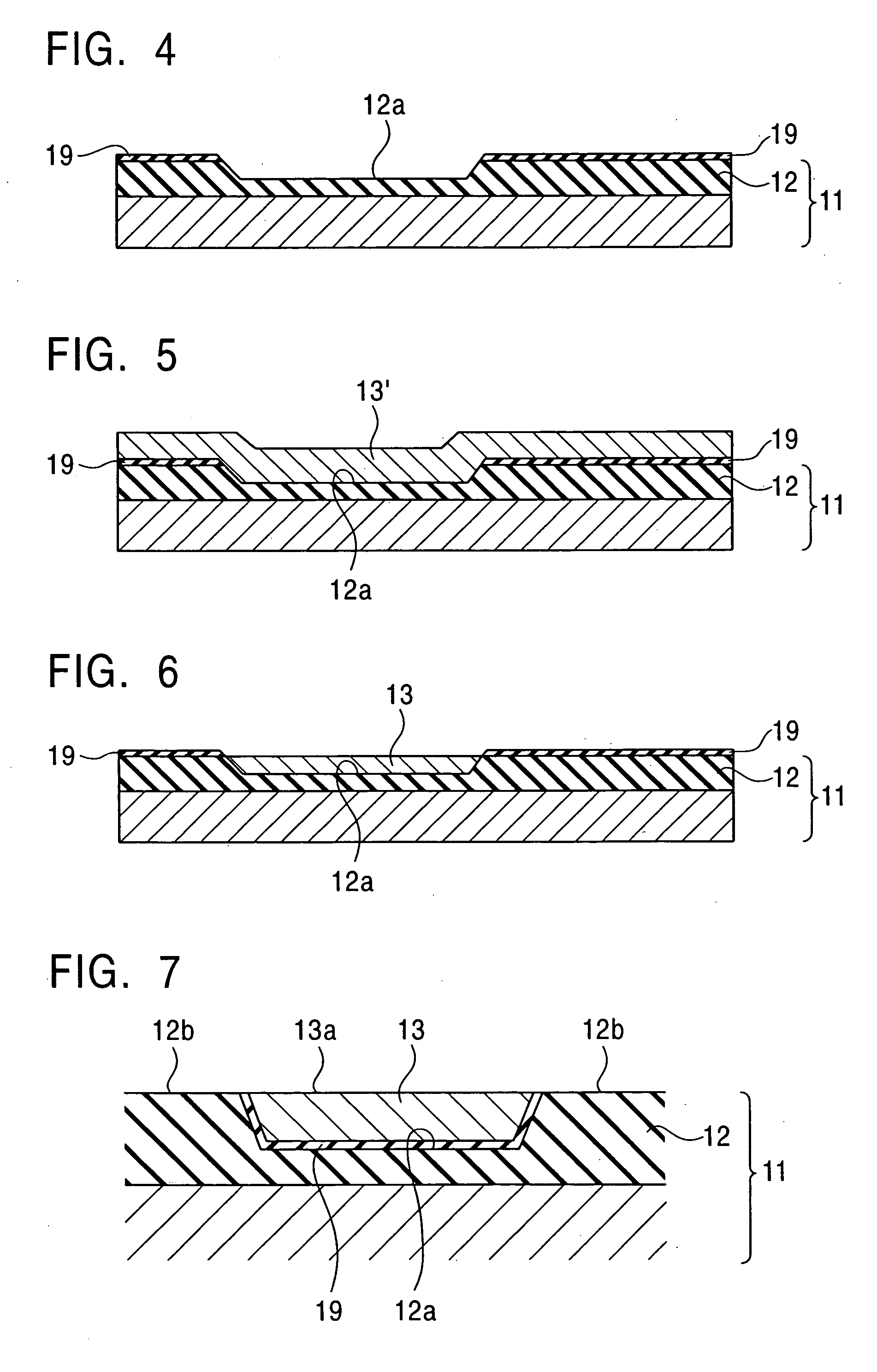
[0027] The thin-film magnetic head 1 has a substrate (AlTiC substrate) 11 made of aluminum-titanium-carbide (AlTiC). On a surface of the AlTiC substrate 11, an underlayer 12 made of alumina is formed as a substrate protective layer in advance.

[0028] On the AlTiC substrate 11, a lower shielding layer 13, a lower gap layer 14, a magnetoresistive sensor 2,...


PUM

PropertyMeasurementUnit
thicknessaaaaaaaaaa
thicknessaaaaaaaaaa
depthaaaaaaaaaa

Abstract

In a thin-film magnetic head having a multilayered film developing a magnetoresistive effect, which is present between an upper shielding layer and a lower shielding layer both formed above an AlTiC substrate, a recess for defining the lower shielding layer is formed in an underlayer present on a surface of the AlTiC substrate, and a lower shielding layer made of NiFe is provided in the recess. A SiO2 film is interposed between the underlayer and the lower shielding layer.

Description

BACKGROUND OF THE INVENTION [0001] 1. Field of the Invention [0002] The present invention relates to a thin-film magnetic head (magnetoresistive head) for reading (and writing) information with high-density recording by utilizing the magnetoresistive effect, and a method of forming the thin-film magnetic head. [0003] 2. Description of the Related Art [0004] A thin-film magnetic head for reproduction includes, in its basic structure, a multilayered film developing the magnetoresistive effect between an upper shielding layer and a lower shielding layer, which are formed above an AlTiC substrate. A thin-film magnetic head is also known which is constituted as a recording / reproducing head by forming, on the thin-film magnetic head for reproduction, a thin-film inductive head for recording (magnetoresistive recording head). Roughly speaking, the thin-film magnetic head for recording and reproduction is constructed by successively forming a lower shielding layer, a lower gap layer, a magn...

Claims


Application Information

Patent Timeline
Patent Type & Authority Applications(United States)
IPC IPC(8): G11B5/31G11B5/39G11B5/40H01L43/08
CPCB82Y10/00Y10T29/49041G11B5/3106G11B5/3133G11B5/3903G11B5/40G11B2005/3996Y10T428/1157Y10T29/49044Y10T29/49032Y10T428/1121Y10T29/49048Y10T428/24612Y10T29/49052B82Y25/00
Inventor SATO, KIYOSHI
Owner TDK CORPARATION
Why Eureka
Try Eureka