Capacitor and semiconductor device and method for fabricating the semiconductor device

a semiconductor device and capacitor technology, applied in the direction of fixed capacitor details, fixed capacitors, printed circuit non-printed electric components association, etc., can solve the problems of insufficient removal of high frequency noise, and insufficient deceleration of source voltage variations, etc., to achieve stable operation, increase the effect of density and larger capacitan

Inactive Publication Date: 2005-07-21
FUJITSU LTD
View PDF15 Cites 15 Cited by
  • Summary
  • Abstract
  • Description
  • Claims
  • Application Information

AI Technical Summary

Benefits of technology

[0027] An object of the present invention is to provide a capacitor which can improve capacitance without lowering voltage resistance, and a semiconductor device with the capacitor, and a semiconductor device having the capacitor.
[0028] Another object of the present invention is to provide a semiconductor device which can meet the requirements of down-sizing and higher density while being able to ensuring stable operation in high-frequency region, and a method for fabricating the semiconductor device.
[0029] According to one-aspect of the present invention, there is provided a capacitor comprising a first conducting film formed on a substrate, a first dielectric film formed on the first conducting film, a second conducting film formed on the first dielectric film, a second dielectric film formed above the second conducting film, covering an edge of the second conducting film, and a third conducting film formed above the second dielectric film, covering a part of the second dielectric film covering the edge of the second conducting film, the capacitor further comprising: an insulation film covering said edge of the second conducting film or said part of the second dielectric film. An effective thickness of the insulation film between the second conducting film and the third conducing film in the region near the edge of the second conducting film can be increased, whereby concentration of electric fields in the region near the edge of the second conducting film. Consequently, the capacitor can have large capacitance without lowering voltage resistance.

Problems solved by technology

Reasons for the lower voltage resistance have not been made clear, and the lower voltage resistance has been a barrier to practicing the proposed capacitor.
When large inductance is present between the LSI and the decoupling capacitor, source voltage variations cannot be sufficiently depressed, and high frequency noises cannot be sufficiently removed.
However, some inductance is present due to the via formed in the circuit wiring substrate, whereby source voltage variations cannot be depressed sufficiently, and high frequency noises cannot be removed sufficiently.
A long wiring pattern is present between the source pins and ground pins of the memory IC, and the decoupling capacitor, which makes it impossible to sufficiently depress source voltage variations and to remove high frequency noises.
However, the decoupling capacitor has a very large thickness, and is not able to satisfy the requirements of down-sizing and higher density.

Method used


Image

  • Capacitor and semiconductor device and method for fabricating the semiconductor device
  • Capacitor and semiconductor device and method for fabricating the semiconductor device
  • Capacitor and semiconductor device and method for fabricating the semiconductor device

Examples


first embodiment

A First Embodiment

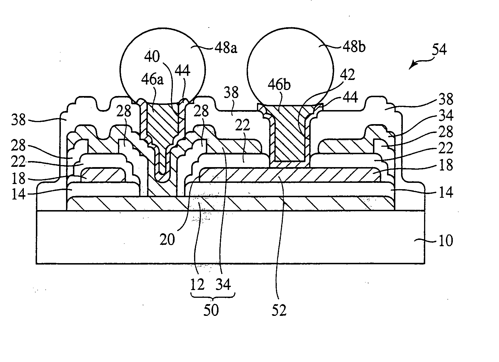
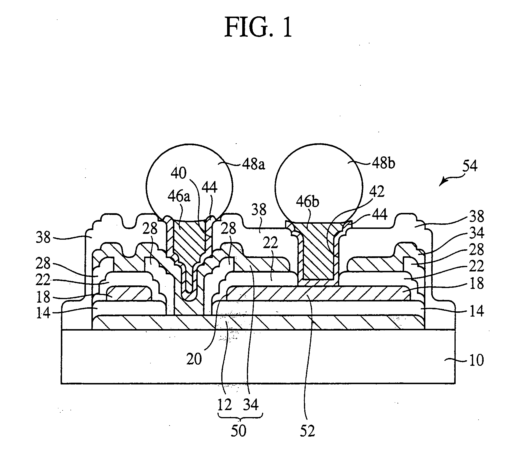
[0082] The principle of the present invention will be explained before the capacitor according to a first embodiment of the present invention is explained.

[0083] The inventors of the present invention made earnest studies of a mechanism for the low voltage resistance of the capacitor shown in FIG. 36 by using the following ideal model of the capacitor.

[0084]FIG. 37A is a schematic view of a part of an ideal model of the capacitor. In FIG. 37A, the part where a conducting film 318 and a conducting film 334 are opposed to each other is three-dimensionally shown. In this model, a dielectric film 322 has a uniform thickness. A potential at the lower end of the conducting film 318 is 0 V, and a potential at the lower end of the conducting film 334 is 1 V.

[0085]FIG. 37B is the sectional view along the plane ABC in FIG. 37A. The conducting film 318 and the conducting film 334 are opposed to each other across the dielectric film 322.

[0086]FIG. 38 is a view of a potenti...

second embodiment

A Second Embodiment

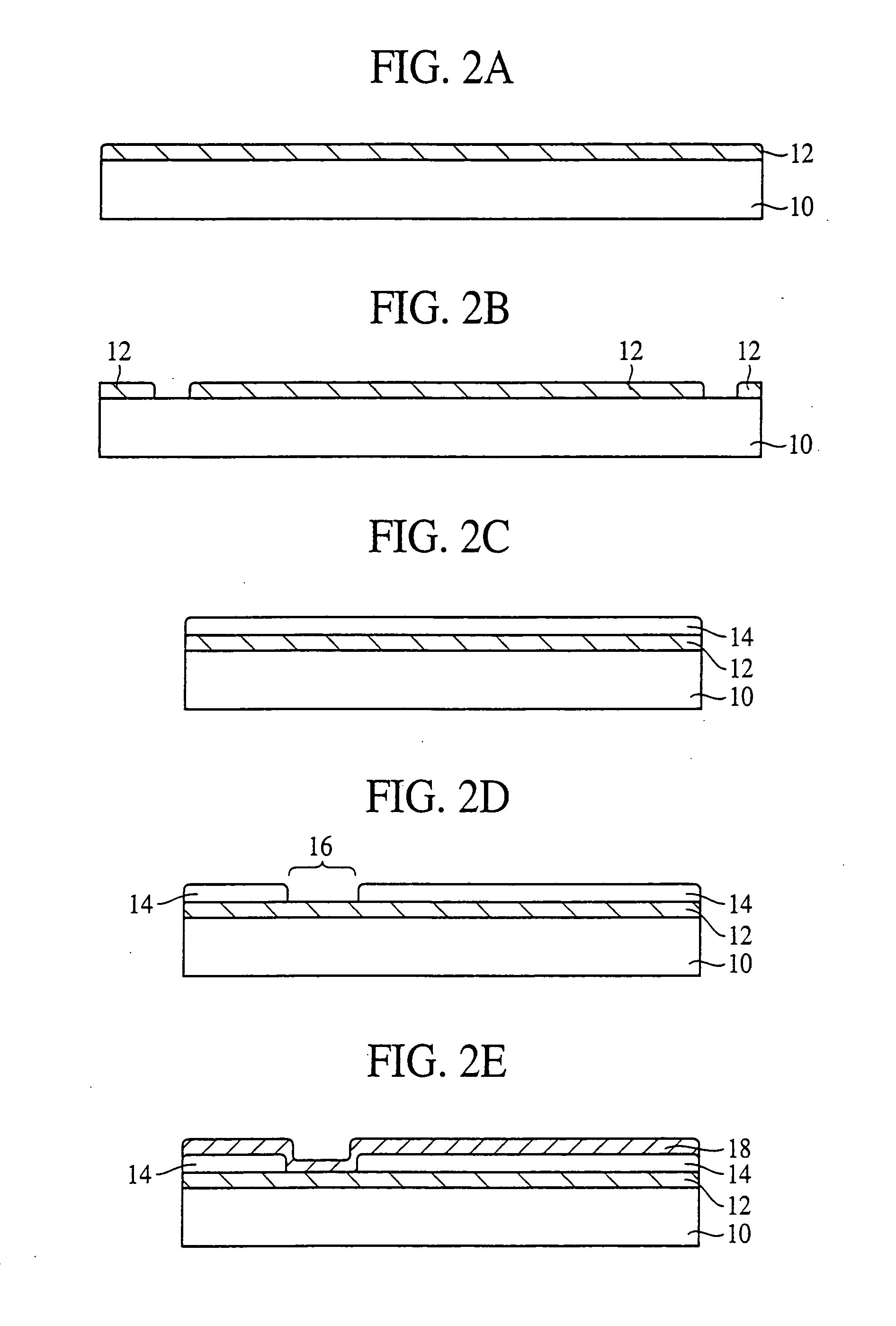
[0133] The capacitor according to a second embodiment of the present invention and the method for fabricating the capacitor will be explained with reference to FIGS. 7 to 10. FIG. 7 is a sectional view of the capacitor according to the present embodiment. FIGS. 8A to 10C are sectional views of the capacitor according to the present embodiment in the steps of the method for fabricating the same, which explain the method. The same members of the present embodiment as those of the capacitor according to the first embodiment and the method for fabricating the capacitor, shown in FIGS. 1 to 6, are represented by the same reference numbers not to repeat or to simplify their explanation.

[0134] (Capacitor)

[0135] The capacitor according to the present embodiment will be explained with reference to FIG. 7.

[0136] As shown in FIG. 7, the capacitor 54a according to the present embodiment is mainly characterized in that an insulation film 28a is formed, covering the edge of ...

third embodiment

A Third Embodiment

[0148] The capacitor according to a third embodiment of the present invention will be explained with reference to FIG. 11. FIG. 11 is a sectional view of the capacitor according to the present embodiment. The same members of the present embodiment as those of the capacitor according to the second embodiment and the method for fabricating the capacitor, shown in FIGS. 1 to 10C are represented by the same reference numbers not to repeat or to simplify their explanation.

[0149] The capacitor 54b according to the present embodiment is characterized mainly in that a dielectric film 56 and a conducting film 66 are formed further on a conducting film 34 so that the electrodes have increased areas for increased capacitance of the capacitor.

[0150] As shown in FIG. 11, a dielectric film 56 of a 200 nm-thickness BST is formed on the conducting film 34. The dielectric film 56 is formed, covering the edge of the conducting film 34.

[0151] In the region near the conducting film...


PUM


Abstract

A capacitor comprises a first conducting film 12 formed on a substrate 10, a first dielectric film 14 formed on the first conducting film, a second conducting film 18 formed on the first dielectric film, a second dielectric film 22 formed above the second conducting film, covering the edge of the second conducting film, a third conducting film 34 formed above the second dielectric film, covering a part of the second dielectric film covering the edge of the second conducting film. The capacitor further comprises an insulation film 28 covering the edge of the second conducing film or the part of the second dielectric film. An effective thickness of the insulation film between the second conducting film and the third conducing film in the region near the edge of the second conducting film can be increased, whereby concentration of electric fields in the region near the edge of the second conducting film. Consequently, the capacitor can have large capacitance without lowering voltage resistance.

Description

BACKGROUND OF THE INVENTION [0001] The present invention relates to a capacitor, and a semiconductor device comprising the capacitor, more specifically to a capacitor using a dielectric thin film, and a semiconductor device comprising the capacitor. [0002] The present invention also relates to a semiconductor device and a method for fabricating the semiconductor device, more specifically to a semiconductor device which can ensure stable operation in high frequency region, and a method for fabricating the semiconductor device. [0003] Generally, a decoupling capacitor is mounted near an LSI (Large Scale Integrated Circuit), etc. mounted on a circuit wiring substrate, for the prevention of erroneous operation due to source voltage variations and high frequency noises. [0004] The substrate of the decoupling capacitor is independent of the circuit wiring substrate and is suitably mounted on the circuit wiring substrate. [0005] Recently, as LSIs, etc. have higher speed and lower power con...

Claims


Application Information

Patent Timeline
Patent Type & Authority Applications(United States)
IPC IPC(8): H01L21/02H01L21/768H01L23/498H01L23/50H01L23/522H01L23/64H01L27/08
CPCH01L21/76885H01L2224/16235H01L23/49822H01L23/50H01L23/5223H01L23/642H01L27/0805H01L28/55H01L2224/16H01L2924/01046H01L2924/01077H01L2924/01078H01L2924/01079H01L2924/15311H01L2924/19103H01L2924/19104H01L2924/3011H01L21/76898H01L2224/16265H01L2224/32265H01L23/3114H01L24/94H01L24/97H01L25/16H01L2224/14051H01L2224/73204H01L2224/94H01L2224/97H01L2924/19041H01L2924/19042H01L2924/14H01L2224/05573H01L2224/05568H01L2924/00014H01L23/481H01L24/05H01L24/06H01L2224/06051H01L2224/14181H01L2224/73259H01L2224/83H01L2224/81H01L2924/00H01L2224/05599H01L2224/1403
Inventor SHIOGA, TAKESHIKARASAWA, KAZUAKIKURIHARA, KAZUAKI
Owner FUJITSU LTD
Why Eureka
Try Eureka