

Method of making toroidal MRAM cells
a technology of toroidal mram cells and mram cells, which is applied in the direction of digital storage, instruments, electrical equipment, etc., can solve the problems of inability to use wafers, and inability to mask the entire substrate at on
- Summary
- Abstract
- Description
- Claims
- Application Information
AI Technical Summary
Problems solved by technology
Method used
Image

Examples
Embodiment Construction
[0035] Before proceeding with the detailed description, it is to be appreciated that the present invention is not limited to use or application with a specific type of magnetic memory. Thus, although the present invention is, for the convenience of explanation, depicted and described with respect to typical exemplary embodiments, it will be appreciated that this invention may be applied with other types of magnetic memory.
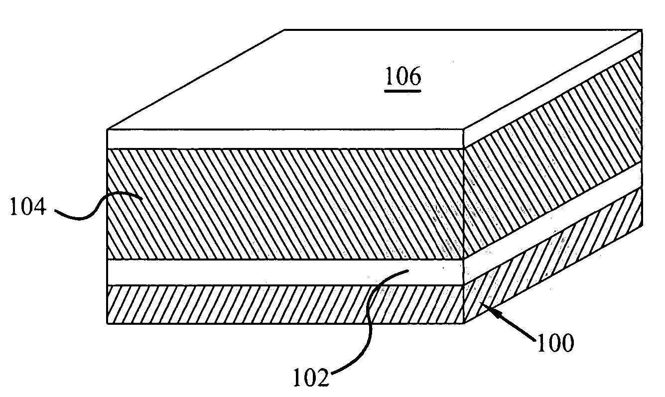
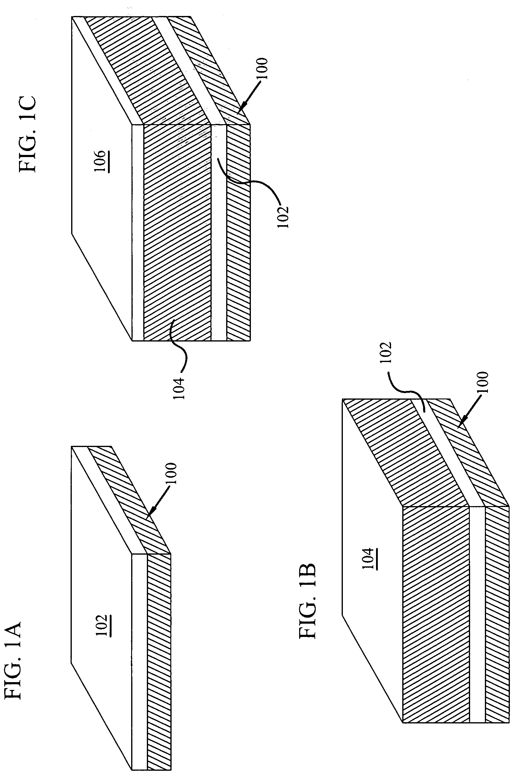
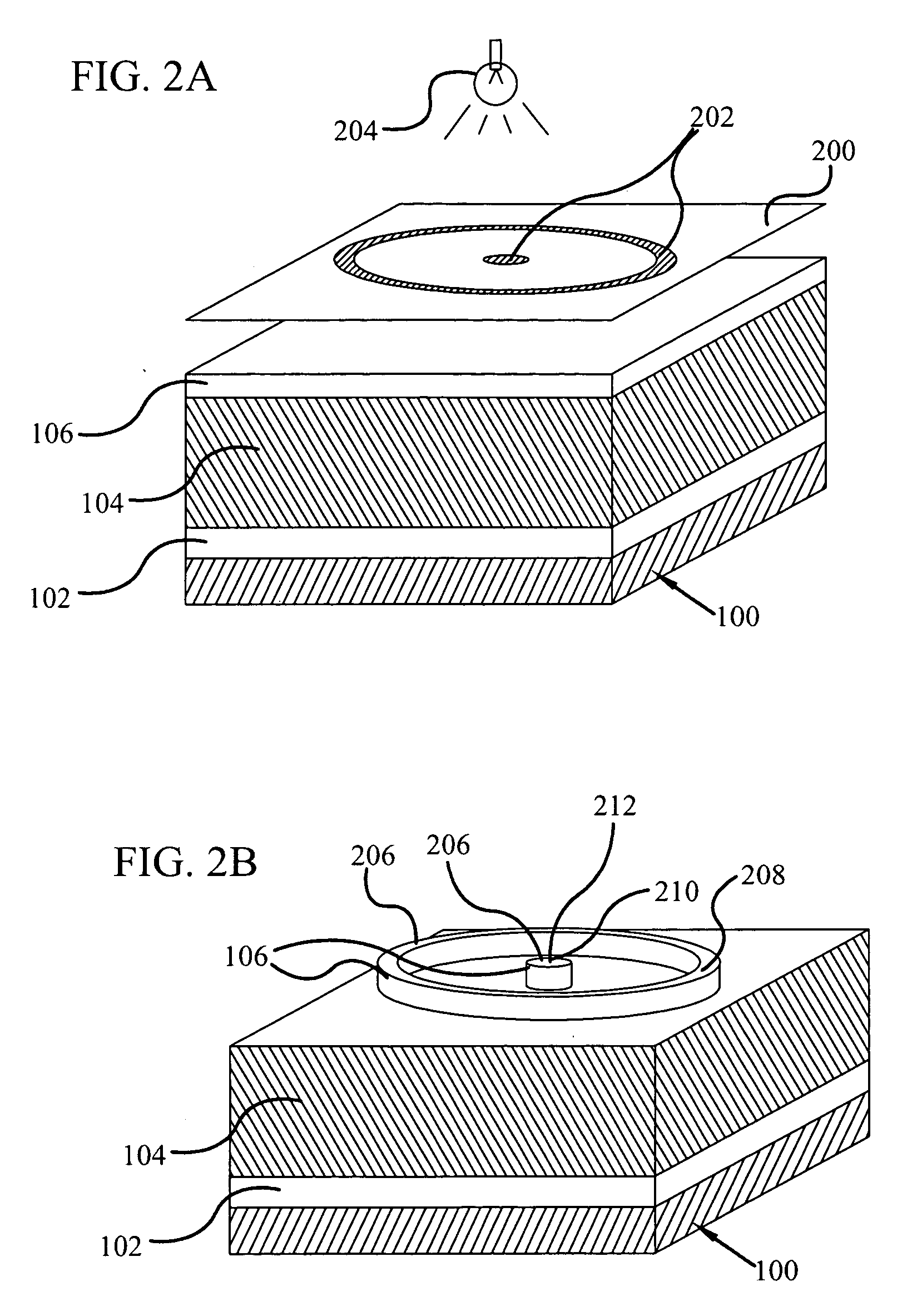
[0036] Referring now to the drawings, FIGS. 1 through 5 conceptually illustrate a method of making a toroidal magnetic memory cell, illustrated in completed form as toroidal magnetic memory cell 512 in FIGS. 5C & 5D), such as may be used in magnetic random access memory (MRAM), according to an embodiment of the present invention. It will be appreciated that the described process need not be performed in the order in which it is herein described, but that this description is merely exemplary of one preferred method of fabricating toroidal magnetic memory cell 512. ...
PUM
 Abstract
Description
Claims
Application Information