Electro-optical device and electronic device

a technology of optical devices and electronic devices, applied in the field of optical devices, can solve the problems of reducing the effective luminescence surface area (effective image display area) of the pixel, unable to avoid, and difficult to ensure the performance required by all circuits and elements, so as to increase the operating performance of the el display device and increase its reliability

Inactive Publication Date: 2005-07-28
SEMICON ENERGY LAB CO LTD
View PDF99 Cites 54 Cited by
  • Summary
  • Abstract
  • Description
  • Claims
  • Application Information

AI Technical Summary

Benefits of technology

[0010] In view of the above conventional technique, an object of the present invention is to provide an electro-optical device having good operation performance and high reliability, and in particular, to provide an EL display device. Another object of the present invention is to increase the quality of electronic equipment (an electronic device) having the electro-optical device as a display by increasing the image quality of the electro-optical device.
[0013] It becomes possible to raise the operating performance of the EL display device, and to increase its reliability, with the present invention by performing proper use of TFTs on the same substrate, as above. Note that the concepts of the present invention are not limited to a pixel portion, and that the present invention is characterized by the point of being able to optimize the TFT structure contained in the pixel portion and in a driver circuit portion for driving the pixel portion.

Problems solved by technology

This is a problem which cannot be avoided because the switching element (T1) is formed by a transistor.
However, the capacitor (Cs) is formed within the pixel, and therefore this becomes a factor in reducing the effective luminescence surface area (effective image display area) of the pixel.
In this type of case, it is difficult to ensure the performance required by all of the circuits and element with only one TFT structure.

Method used


Image

  • Electro-optical device and electronic device
  • Electro-optical device and electronic device
  • Electro-optical device and electronic device

Examples


embodiment 1

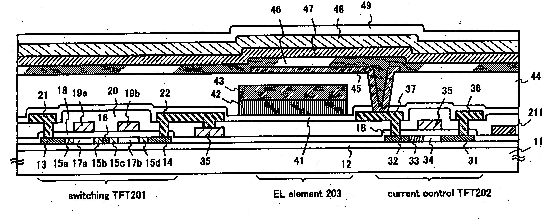
[0107] The embodiments of the present invention are explained using FIGS. 3A to 5C. A method of manufacturing a pixel portion, and TFTs of a driver circuit portion formed in the periphery of the pixel portion, is explained here. Note that in order to simplify the explanation, a CMOS circuit is shown as a basic circuit for the driver circuits.

[0108] First, as shown in FIG. 3A, a base film 301 is formed with a 300 nm thickness on a glass substrate 300. Silicon oxynitride films are laminated as the base film 301 in embodiment 1. It is good to set the nitrogen concentration to between 10 and 25 wt % in the film contacting the glass substrate 300.

[0109] Further, it is effective to form a heat radiating layer, made from the same material as that of the first passivation film 41 shown in FIG. 1, as a portion of the base film 301. A large electric current flows in a current control TFT, heat is easily generated, and therefore it is effective to form the heat radiating layer as close as po...

embodiment 2

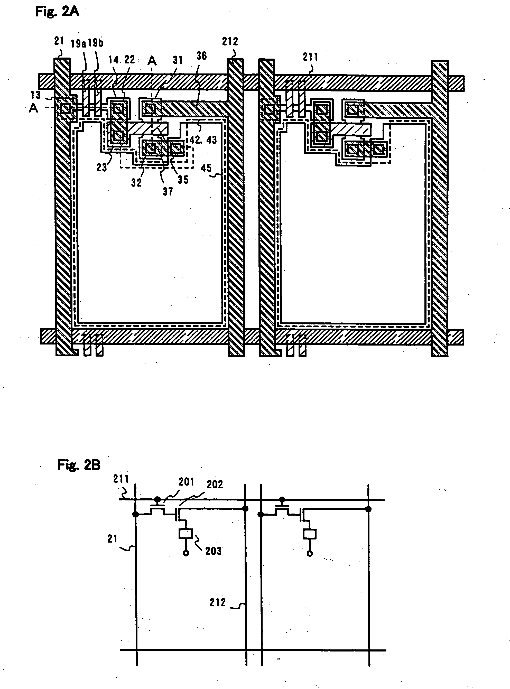
[0196] In embodiment 2, an example of a pixel constitution is shown in FIG. 10 which differs from the constitution shown in FIG. 2B.

[0197] The two pixels shown in FIG. 2B are arranged with symmetry around the current supply line in embodiment 2. Namely, as shown in FIG. 10, by making the current supply line 213 common between the two pixels neighboring the current supply line, the number of wirings needed can be reduced. Note that the structure of the TFTs placed inside the pixels may be left as is.

[0198] If this type of constitution is used, then it becomes possible to manufacture a very high definition pixel portion, increasing the image quality.

[0199] Note that the constitution of embodiment 2 can easily be realized in accordance with the manufacturing processes of embodiment 1, and that the explanations of embodiment 1 and of FIG. 1 may be referenced regarding points such as the structure of the TFTs.

embodiment 3

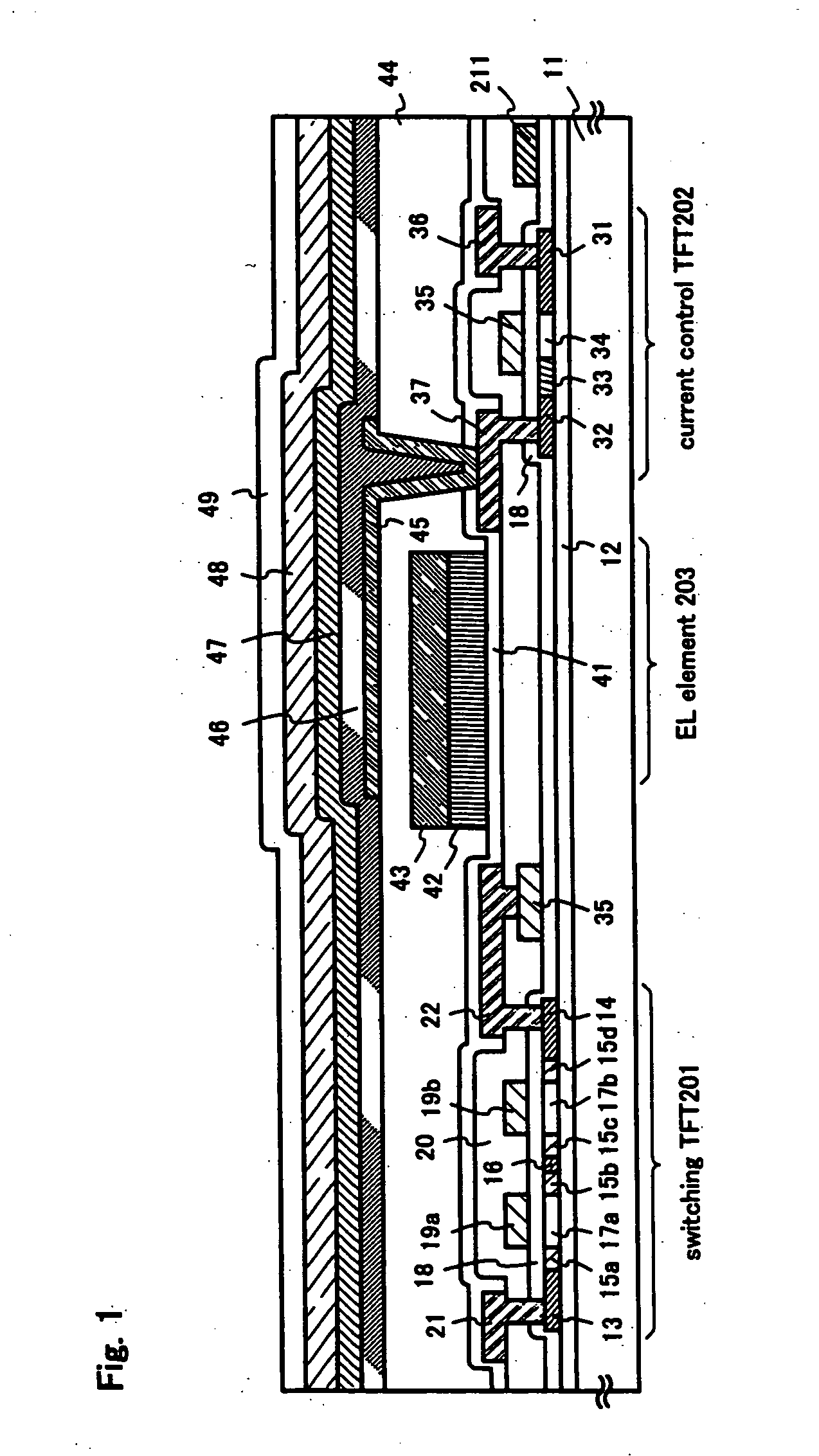
[0200] A case of forming a pixel portion having a structure which differs from that of FIG. 1 is explained using FIG. 11 in embodiment 3. Note that processes up through the formation of the second interlayer insulating film 44 may be performed in accordance with embodiment 1. Furthermore, the structures of the switching TFT 201 and the current control TFT 202, covered by the second interlayer insulating film 44, are the same as those of FIG. 1, and their explanation is therefore omitted.

[0201] In the case of embodiment 3, a pixel electrode 51, a cathode 52, and an EL layer 53 are formed after forming a contact hole in the second interlayer insulating film 44 and the first passivation film 41. The cathode 52 and the EL layer 53 are formed in succession, without exposure to the atmosphere, by vacuum evaporation in embodiment 3, and at that time a red color emitting EL layer, a green color emitting EL layer, and a blue color emitting layer are formed selectively in separate pixels by ...


PUM


Abstract

An object of the present invention is to provide an EL display device having a high operation performance and reliability. The switching TFT 201 formed within a pixel has a multi-gate structure, which is a structure which imposes an importance on reduction of OFF current value. Further, the current control TFT 202 has a channel width wider than that of the switching TFT to make a structure appropriate for flowing electric current. Morever, the LDD region 33 of the current control TFT 202 is formed so as to overlap a portion of the gate electrode 35 to make a structure which imposes importance on prevention of hot carrier injection and reduction of OFF current value.

Description

BACKGROUND OF THE INVENTION [0001] 1. Field of the Invention [0002] The present invention relates to an electro-optical device, typically an EL (electroluminescence) display device formed by a semiconductor element (an element using a semiconductor thin film) made on a substrate, and to electronic equipment (an electronic device) having the electro-optical device as a display (also referred to as a display portion). [0003] 2. Description of the Related Art [0004] Techniques of forming a TFT on a substrate have been widely progressing in recent years, and developments of applications to an active matrix type display device are advancing. In particular, a TFT using a polysilicon film has a higher electric field effect mobility (also referred to as mobility) than a TFT using a conventional amorous silicon film, and high speed operation is therefore possible. As a result, it becomes possible to perform pixel control, conventionally performed by a driver circuit external to the substrate...

Claims


Application Information

Patent Timeline
Patent Type & Authority Applications(United States)
IPC IPC(8): H01L21/77H01L27/12H01L27/32H01L29/423H01L29/786H01L51/52H05B33/04
CPCH01L27/322H01L27/1255H01L27/3248H01L27/3262H01L29/42384H01L29/78621H01L29/78627H01L29/78645H01L29/78696H01L51/5237H01L51/524H01L51/5246H01L51/5259H01L51/529H01L2251/5315H01L33/08H01L2924/0002H01L27/3244H01L27/1218H01L2924/00H10K59/38H10K59/123H10K59/12H10K59/1213H10K50/841H10K50/846H10K50/8426H10K50/87H10K2102/3026H10K59/127H10K50/84
Inventor YAMAZAKI, SHUNPEIKOYAMA, JUNYAMAMOTO, KUNITAKAKONUMA, TOSHIMITSU
Owner SEMICON ENERGY LAB CO LTD
Why Eureka
Try Eureka