Flip chip assemblies and lamps of high power GaN LEDs, wafer level flip chip package process, and method of fabricating the same

a technology of flip chip and high power gan leds, which is applied in the direction of electrical apparatus, semiconductor devices, semiconductor/solid-state device details, etc., to achieve the effects of reducing current crowding effect, fast thermal dissipation, and high light extraction

Inactive Publication Date: 2005-07-28
PENG HUI +1
View PDF5 Cites 16 Cited by
  • Summary
  • Abstract
  • Description
  • Claims
  • Application Information

AI Technical Summary

Benefits of technology

[0023] The primary object of the present invention is to provide new flip chip assemblies and lamps for high power semiconductor chips or devices including GaN LEDs to have fast thermal dissipation, higher light extraction, and reduced current crowding effect.
[0024] The second object of the present invention is to provide a new wafer level flip chip package process for cost effectively manufacturing the flip chip assemblies of high power semiconductor chips or devices including GaN LEDs with high throughput.
[0025] The third object of the present invention is to provide new flip chip assemblies and lamps of semiconductor chips or devices to significantly improve the extraction efficiency by eliminating both the totally internal reflection and the Fresnel reflection at the dome-air interface.
[0026] The fourth object of the present invention is to provide new flip chip assemblies of semiconductor chips or devices to eliminate the lattice mismatch to improve the internal efficiency.

Problems solved by technology

Secondly, removing the sapphire or GaN substrate of the bonded LED wafer.
Thirdly disposing a patterned electrical contact pad to the epitaxial layer that previously contacted to the removed substrate.

Method used


Image

  • Flip chip assemblies and lamps of high power GaN LEDs, wafer level flip chip package process, and method of fabricating the same
  • Flip chip assemblies and lamps of high power GaN LEDs, wafer level flip chip package process, and method of fabricating the same
  • Flip chip assemblies and lamps of high power GaN LEDs, wafer level flip chip package process, and method of fabricating the same

Examples


Embodiment Construction

[0051] While embodiments of the present invention will be described below, those skilled in the art will recognize that other assemblies, lamps and processes are capable of implementing the principles of the present invention. Thus the following description is illustrative only and not limiting.

[0052] Reference is specifically made to the drawings wherein like numbers are used to designate like members throughout.

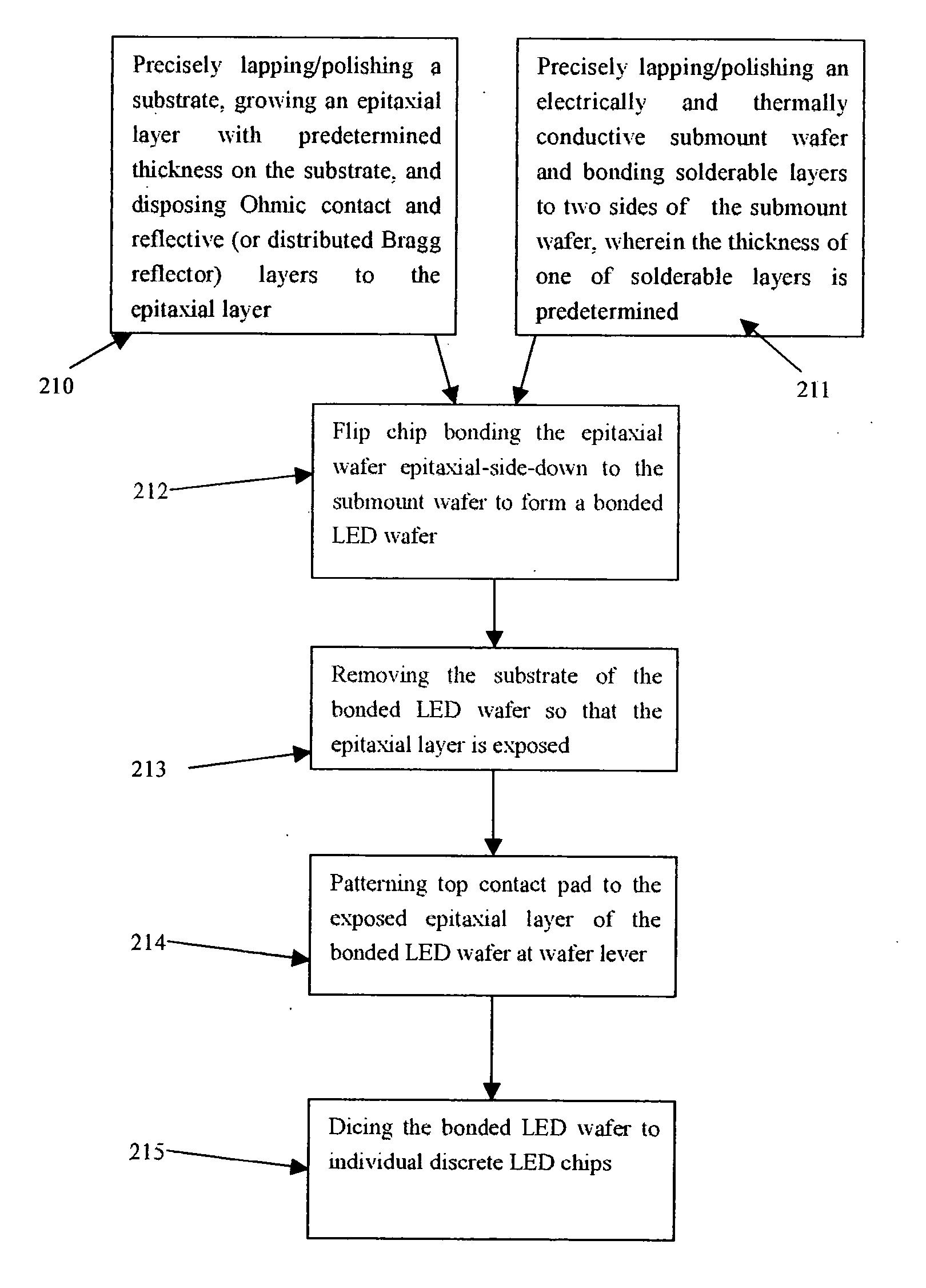
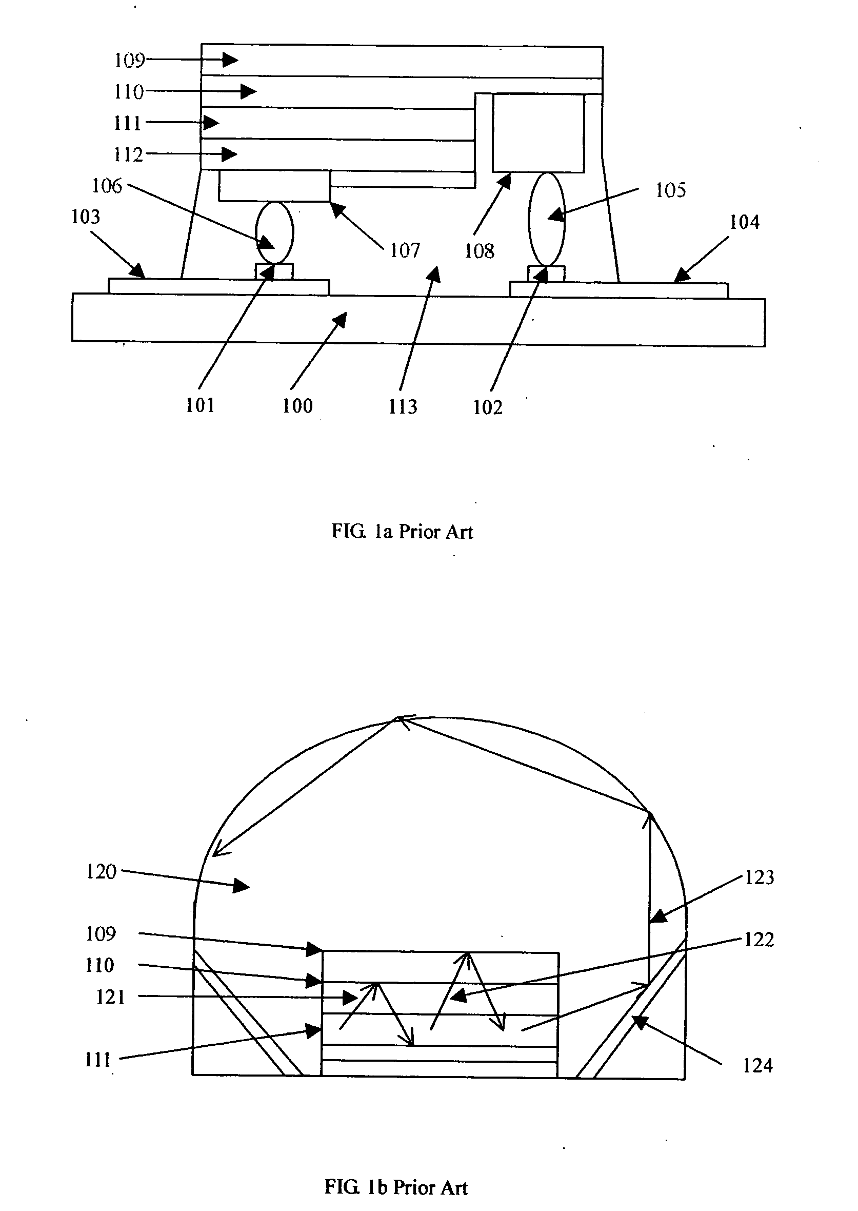
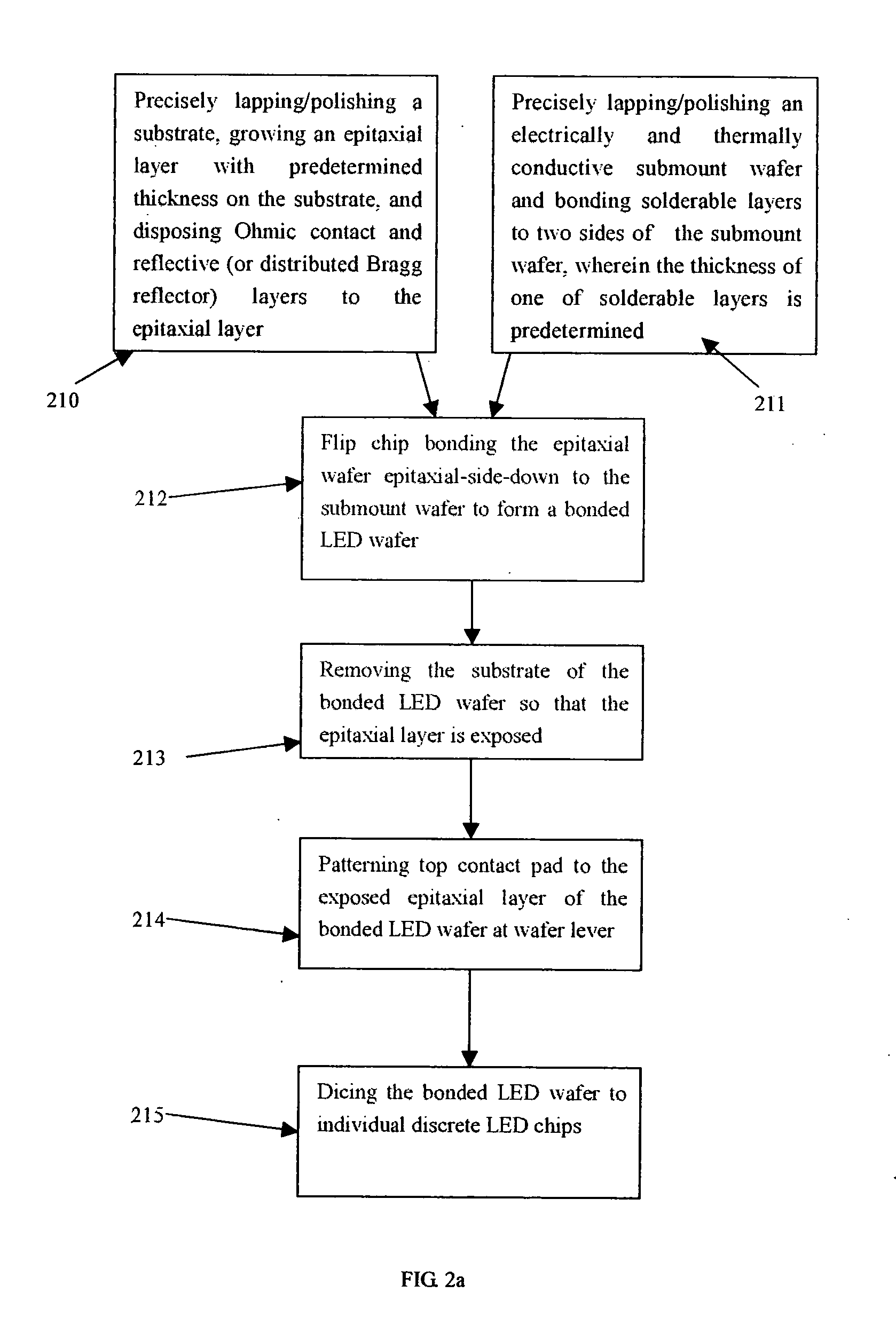
[0053] Note the followings: [0054] (1) The dimensions of all of drawings are not to scale. [0055] (2) GaN LEDs as embodiments of the present invention are illustrated in the FIG. 2 to FIG. 4. However the same flip chip assemblies and package process are applicable to other semiconductor chips or devices. [0056] (3) Although a sapphire substrate has been used in FIG. 2 to FIG. 4, for GaN LEDs, the substrate may be GaN. Also Si wafer has been tried for growing GaN LEDs. The flip chip package process of the present invention is applicable for GaN LEDs with Si substrate. Actu...


PUM


Abstract

The present invention discloses new flip chip assemblies and lamps for high power semiconductor chips or devices including GaN LEDs and a new wafer level flip chip packaging process for cost effectively manufacturing the same. The advantages of the new flip chip assemblies, lamps, and the wafer level flip chip package process are: (1) the fabricating process is simpler; (2) no need for expensive flip chip equipments; (3) the throughput is higher; (4) eliminating lattice mismatch between the substrate and the epitaxial layer by removing the substrate; (5) better thermal dissipation; (6) reduced current crowding effect and higher current density; (7) higher light extraction efficiency; (8) eliminating the totally internal reflection; and (9) eliminating the Fresnel reflection at the dome-air interface.

Description

BACKGROUND OF THE INVENTION [0001] (1) Field of the Invention [0002] The present invention relates to new flip chip assemblies and lamps of high power semiconductor chips or devices including high power GaN LEDs and a new wafer level flip chip package process for fabricating the same. [0003] (2) Prior Art [0004] The chip level flip chip package process, especially for high power GaN LEDs, has following issues: (1) the process is complicate, packaging equipments are expensive, and the throughput is low, which are the bottlenecks for the fabrication of flip chip assemblies of high power GaN LEDs; (2) the limited thermal dissipation due to the usage of organic underfill materials; (3) the lattice mismatch still existing for GaN LEDs with a sapphire substrate; and (4) the totally internal reflection causing low extraction efficiency. [0005] The chip level flip chip package process of prior art comprises the following steps: disposing bumps with accurate position, size, and height onto a...

Claims


Application Information

Patent Timeline
Patent Type & Authority Applications(United States)
IPC IPC(8): H01L21/00H01L21/44H01L23/02H01L29/40H01L33/00H01L33/38H01L33/62
CPCH01L33/0079H01L33/38H01L33/62H01L2224/16H01L2924/01004H01L2924/01079H01L2224/48091H01L2924/10253H01L2924/12041H01L2924/00014H01L2924/00H01L2224/05573H01L2224/05568H01L2224/16238H01L24/05H01L2224/0603H01L2224/06102H01L2224/1703H01L33/0093H01L2224/05599
Inventor PENG, HUIPENG, GANG GRANT
Owner PENG HUI
Why Eureka
Try Eureka