Power converter, power system provided with same, and mobile body
Inactive Publication Date: 2005-07-28
HITACHI LTD
13 Cites 30 Cited by
AI-Extracted Technical Summary
Problems solved by technology
Therefore, it is considered that in the above-mentioned mounting method, the difference of linear expansion coefficients between the Hall element and the resin formed body causes thermal stress, which results in permanent deformation of the Hall element, thereby decreasing the accuracy of the current detector.
However, in this mounting method, i...
Method used
[0238] According to this embodiment, a current detector 40, which detects current flowing through the detection conductor 41 by inputting magnetic flux generated by the detection conductor 41 directly into the magnetic detecting semiconductor element 43, is incorporated into a power converter 24, and therefore, it is possible to make the current detector 40 smaller than conventional current detectors, thereby enabling the current detector 40 to be built in the power module 16 of the power converter 24. Therefore, according to this embodiment, no space is necessary in the power converter 24 to install the current detector, an AC bus bar 31B can be short or eliminated, an AC terminal block 35B can be eliminated, and the cable for supplying electric power to the motor 5 can be directly connected to the connection terminal 15; as a consequence, a power converter 24 can be made small. Also, according to this embodiment, it is possible to inhibit the size of the power module 16 from becoming large.
[0239] Furthermore, according to this embodiment, relative distance between the detection conductor 41 and the power module base 27 is larger than relative distance between the current detection electrode 42, which is installed on the power module base 27 with the ceramic substrate 28 interposed, and the power module base 27 (i.e. larger than relative distance between the power controlling semiconductor element 7 and the power module base 27), thereby making it possible to inhibit the influence of the magnetic flux which is generated by eddy current (induction current) flowing through the power module base 27 as the result that the magnetic flux generated by the current flowing through the detection conductor 41 interlinks with the power module base 27. Therefore, according to this embodiment, it is possible to improve the accuracy of the current detector 40. That is, the extent to which the amount of magnetic flux generated by the current flowing through the detection conductor 41 interlinks with the power module base 27 varies depending on the value of the coefficient of magnetically coupling between the magnetic flux generated by current flowing through the detection conductor 41 and the power module base 27. Accordingly, the magnitude of the eddy current (induction current) changes in proportion to the coupling coefficient. For this reason, as relative distance between the detection conductor 41 and the power module base 27 becomes larger, the amount of leakage of magnetic flux generated by current flowing through the detection conductor 41 increases, thereby making the coupling coefficient smaller. This reduces eddy current (induction current), that is, mirror current; therefore, it is possible to inhibit the influence of magnetic flux which is generated as the result of the flowing eddy current (induction current). Consequently, according to this embodiment, it is possible to improve the accuracy of the current detector 40.
[0241] Furthermore, according to this embodiment, at least a part of the magnetic detecting unit 47 is contained in the depression 46 created in the detection conductor 41, and therefore, it is possible to keep an interval between the magnetic detecting semiconductor element 43 and the detection conductor 41 constant. Therefore, according to this embodiment, there is no unevenness between the magnetic detecting semiconductor element 43 and the detection conductor 41, which prevents the accuracy of the current detector 40 from decreasing. Furthermore, the magnetic detecting unit 47 can be easily positioned. Consequently, according to this embodiment, it is possible to prevent production yield from decreasing, thereby preventing production costs of the power converter 24 from increasing.
[0242] Furthermore, according to this embodiment, a detection conductor 41 having a magnetic detecting unit 47 is installed on the power module base 27 with the current detection electrode 42 and ceramic substrate 28 interposed. This configuration allows heat generated in the detection conductor 41 and the current detection electrodes 42 due to current flow to be discharged via a power module base 27 which is a heat discharge member. Therefore, according to this embodiment, it is possible to inhibit heat transfer to the magnetic detecting unit 47, thereby preventing the temperature of the magnetic detecting semiconductor element 43 from rising above the specification limit. As a result, it is possible to inhibit performance of the magnetic detecting semiconductor element 43 from deteriorating due to heat, thereby increasing the accuracy of the current detector 40. Furthermore, it is possible to inhibit permanent deformation from occurring in the magnetic detecting semiconductor element 43 due to thermal stress generated by the difference of linear expansion coefficients between the magnetic detecting semiconductor element 43 and the molded resin 45, thereby increasing the accuracy of the current detector 40.
[0244] Furthermore, according to this embodiment, it is possible to install a magnetic detecting unit 47 susceptible to thermal deformation separately from a detection conductor 41 on the power module 16. First, by means of the soldering process in which for several minutes at a high temperature a power controlling semiconductor element 7 is soldered, a detection conductor 41 is soldered onto the electrode 52 of the ceramic substrate 28. After that, a magnetic detecting unit 47 is inserted into a depression 46 created in the detection conductor 41, and a protruding portion 49 is abutted on the molded resin 45, which is not opposite to the depression 46 in the magnetic detecting unit 47, with an adhesion layer 50 interposed, and then the magnetic detecting unit 47 is fixed to the detection conductor 41. Consequently, according to this embodiment, the soldering process is not necessary to mount the magnetic detecting unit 47 to the detection conductor 41, thereby preventing reliability and accuracy of the detection of the magnetic detecting unit 47 from decreasing due to thermal stress caused by the soldering process.
[0245] Furthermore, according to this embodiment, a current detector 40 having a function to calibrate accuracy of the detection is used and the calibration signal for instructing calibration is created by a computer; therefore, it is possible for the computer 9 to calibrate a detection error resulted from misalignment between the magnetic detecting unit 47 and the detection conductor 41 which occurs when the power converter 24 is assembled and a detection error by the current detector 40 resulted from an error caused by the control power source 36. Therefore, according to this embodiment, it is possible to prevent yield of the power module 16 and power converter 24 from decreasing due to initial failure of the current detector 40. Herein, rightly, even if the current detector 40 does not have a function to calibrate accuracy of the detection, a control unit 26, not shown, can have a correction circuit or a computer 9 can execute digital corrections.
[0246] Furthermore, according to this embodiment, a computer other than computer 9 is provided to verify data calibrated by computer 9, thereby further increasing reliability of the current detector 40.
[0253] Furthermore, according to this embodiment, the laminated wiring sheets 54 are disposed together with a wide shield electrode which is wired on the same wiring layer and allows most of the laminated wiring sheets 54 to overlap in a different wiring layer; or, some of the laminated wiring sheets 54 are arranged on different wiring layers, and the laminated wiring sheets 54 are also disposed such that they overlap with the entire area. Accordingly, it is possible to reduce magnetic flux (noise) which interlinks with the electrical annular wire connection created by circuit wiring of the control board 55, and therefore, it is possible to dispose noise control parts, such as a chip capacitor 56, in proximity to the magnetic detecting semiconductor element 43. As a result, according to this embodiment, the accuracy of the current detector 40 can be increased.
[0257] According to this embodiment, the same effect as the first embodiment can be obtained, and by integrating a resin formed body 57, which is blended with magnetic powder, and a detection conductor 41 into a magnetic circuit on the resin formed body 57, it is possible to improve the amount of magnetic flux inputted into the magnetic detecting unit 47. Therefore, according to this embodiment, detection sensitivity of the current detector 40 can be increased.
[0260] According to this embodiment, the same effect as the first embodiment can be obtained, and it is possible to prevent magnetic flux generated by the detection current flow from decreasing as the result of the magnetic flux interlinking with the electrical annular wire connection which is created by connection terminals 44 disposed in proximity to one another on the detection conductor 41 and the circuit wiring of the control board 55. Therefore, according to this embodiment, the accuracy of the current detector 40 can be increased.
[0264] According to this embodiment, the same effect as the first embodiment can be obtained, and electrodes 52 and the current detector 40 are bilaterally symmetric with respect to the bisector of the ceramic substrate 28, and hour-glass shaped portions 61 are disposed on the electrodes 52 so that those portions are bilaterally symmetric with respect to the bisector. Therefore, it is possible to control detection current flowing through the detection conductor 41 so that the distribution of the detection current is bilaterally symmetric with respect to the bisector. As a result, according to this embodiment, it is possible to inhibit the current density in the detection conductor 41 from becoming inconsistent due to the current concentration in the complicated wiring of the power module 16 resulting from reducing the size of the power module 16. Consequently, the accuracy of the current detector 40 can be increased.
[0269] According to this embodiment, the wiring on the self and other layers which are in proximity to the detection conductor 41 and the magnetic detecting unit 47 is eliminated, and an engraved portion 63 is provided in the power module base 27 which corresponds to the detection conductor 41 and the magnetic detecting unit 47. Therefore, it is possible to inhibit magnetic flux generated by detection current from being offset by counteracting magnetic flux generated by eddy current flowing through the wiring conductor, ceramic substrate 28 connecting solder 51 and the power module base 27 as the result that magnetic flux generated by detection current interlinks with a wiring conductor other than the detection conductor, ceramic substrate 28 connecting solder 51, and the power module base 27. As a result, according to this embodiment, the accuracy of the current detector can be increased.
[0274] According to this embodiment, the same effect as the first embodiment can be obtained, and connection terminals 44 of the magnetic detecting unit 47 are not directly connected to the control board 55. Therefore, it is possible to flexibly route an aluminum wire 32 or a wire in the power module 16 connected to the aluminum wire 32 and to flexibly lay out the position of the connection with the control board 55 regardless of the location of the current detection unit 47. As a result, distance between the magnetic detecting unit 47 and the detection conductor 41 can be effectively accurate.
[0277] According to this embodiment, because a current detector 40 is provided in the part of the out-going electrode 69 of the AC terminal block 35B, it is not necessary to provide new exclusive wiring for the curr...
Benefits of technology
[0028] According to the aforementioned power converter, a current detector, which detects current flowing through the conductor by inputting magnetic flux generated by the conductor directly into the magnetic detecting semiconductor element, is incorporated, and therefore, it is possible to make the current detector smaller than conventional current detectors, thereby enabling the current detector to be built in the power module of the power converter. Therefore, according to the aforementioned power converter, no space is necessary in the power converter to install the current detector, thereby making the power converter small. Also, according to the aforementioned power converter, it is possible to inhibit the size of the power module from becoming large.
[0029] Furthermore, according to the aforementioned power converter, because the magnetic detecting unit is disposed in the conductor portion or in the vicinity of the conductor portion, relative distance of which to the conductive member is larger than relative distance between the conductor portion laminated on the conductive member with the insulation member interposed and the conductive member, the magnetic flux generated by the current flowing through the conductor interlinks with the conductive member. Therefore, it is possibl...
Abstract
To provide a power converter equipped with a current detector which is small and can carry out highly accurate current detection, in the power converter equipped with a power module 16 having a power controlling semiconductor element 7 disposed on the power module base 27 with a ceramic substrate 28 interposed, and a control unit 26 for controlling the operation of the power controlling semiconductor element 7, a current detector 40 having a magnetic detecting unit 47 which is disposed in the detection conductor 11, electrically connected to the power controlling semiconductor element 7 and disposed on the power module base 27 with the ceramic substrate 28 interposed, and has a magnetic detecting semiconductor element 43 electrically connected to the control unit 26 is provided in the power module 16; and relative distance between the detection conductor 11 and the power module base 27 is larger than the relative distance between the current detection electrode 42 and the power module base 27.
Application Domain
Electronic commutation motor controlMotor/generator/converter stoppers +9
Technology Topic
Power controlEngineering +7
Image
Examples
- Experimental program(20)
Example
[0205] A first embodiment of the present invention will be explained by referring to FIGS. 1 through 9. What is explained as an example in this embodiment is a power converter (inverter) which is incorporated in a motor drive system of an electric car that is driven by a motor as the vehicle's only drive source, and which converts DC power outputted from a battery, which is a power storage means, into three-phase AC power and supplies the power to the motor.
[0206]FIG. 9 is a schematic diagram showing the configuration of an electric car equipped with a motor drive system which incorporates a power converter according to this embodiment. In FIG. 9, 18 denotes a vehicle body. At the front of the vehicle body 18, front wheels having an axle 20 and wheels 19a and 19b attached to both ends of the axle 20 are rotatably mounted. At the rear of the vehicle body 18, rear wheels having an axle 22 and wheels 21a and 21b attached to both ends of the axle 22 are rotatably mounted.
[0207] A motor 5 is mechanically connected to the axle 20 via a gear 23. A power converter 24 is electrically connected to the motor 5, and DC power supplied from a battery 6 is converted into three-phase AC power and supplied. A higher-level control device 25 is electrically connected to the power converter 24, and command signals, such as a response to pressing down the accelerator, are inputted.
[0208]FIG. 8 shows the configuration of a motor drive system of an electric car which incorporates a power converter according to this embodiment. A power converter according to this embodiment is a pulse width modulation system which controls switching operations (ON/OFF operation) of a power controlling semiconductor element 7 according to the PWM signal (pulse width modulation signal) and converts DC power outputted from a battery 6 into three-phase AC power and supplies it to the motor 5. The power converter consists of a power module 16 and a control unit 26.
[0209] The power module 16 is a converter unit which converts DC power outputted from a battery 6 into three-phase AC power and is equipped with a power controlling semiconductor element 7 and a current detector 40. As a power controlling semiconductor element 7, a switching element which is a combination of IGTB and diode element, or a switching element constituted by MOS-FETs is used. The current detector 40 detects current flowing through a current-carrying conductor by inputting magnetic flux generated by the current-carrying conductor directly into a magnetic detecting semiconductor element. The current detector 40 is provided for each phase of current to detect each phase (U-phase, V-phase and W-phase) of three-phase AC power which has been converted by the power controlling semiconductor element 7.
[0210] The control unit 26 controls switching operations (ON/OFF operation) of the power controlling semiconductor element 7 installed in the power module 16 according to the command signal sent by the higher-level control device 25. The control unit 26 has a drive circuit 8, computer 9, control power source 36 and an interface circuit 37.
[0211] The interface circuit 37 receives a command signal, such as a response to pressing down the accelerator, outputted from a higher-level control device 25. The interface circuit 37 has a communication receiver IC39A which receives command signals inputted from a higher-level control device 25 via an input port 38 and a photo coupler 39B which insulates signals outputted from the communication receiver IC39A.
[0212] The computer 9 is constituted by a computing element typified by a microcomputer chip, and carries out arithmetic operations according to a signal outputted by an interface circuit 37 and a detection signal outputted by a current detector 40 and creates and outputs a PWM control signal.
[0213] The drive circuit 8 steps up or down the PWM control signal outputted from the computer 9 and outputs the signal to the power module 16 as a drive signal for controlling switching operations (ON/OFF operation) of the power controlling semiconductor element 7 provided in the power module 16.
[0214] The control power source 36 supplies drive power to the drive circuit 8, computer 9, current detector 40 and interface circuit 37. The control power source 36 has a regulator IC which is a voltage control element for stepping up or down voltage of DC power supplied by the battery 6, a capacitor which is a capacitance element for stabilizing the output of the regulator IC, a transformer which is a voltage control element for creating a power source insulated from the battery 6 and is equipped with a primary winding and secondary winding, a means for changing voltage of the transformer's primary winding according to voltage of the secondary winding, and a diode and a capacitor 3 which are a rectifying element and a capacitance element, respectively, for smoothing the output of the transformer's secondary winding.
[0215] The DC power supplied from the battery 6 is inputted into the power module 16 via a DC bus bar 31A supported by the DC terminal block 35A. On the other hand, a command signal, such as a response to pressing down the accelerator, is inputted into the control unit 26 from the higher-level control device 25 and is inputted into the computer 9 via the interface circuit 37 together with the detection signal outputted from the current detector 40. The computer 9 carries out arithmetic operations according to the inputted signal, creates a PWM control signal and outputs the signal to the drive circuit 8. The drive circuit 8 steps up or down the PWM control signal and then inputs it as a drive signal into the power module 16. This controls switching operations of the power controlling semiconductor element 7, thereby converting DC power inputted into the power module 16 into three-phase AC power. The converted three-phase AC power is supplied to the motor 5 via an AC bus bar 31B supported by the AC terminal block 35B. The motor 5 is driven by the supplied three-phase AC power.
[0216]FIGS. 4 and 5 show the configuration of one-phase portion of the power module which is incorporated in a power converter according to this embodiment. FIG. 6 shows the electrical circuit configuration of one-phase portion of the power module which is incorporated in a power converter according to this embodiment. FIG. 7 shows the entire configuration of the power converter according to this embodiment.
[0217] In the drawings, 30 denotes a power converter case. The power converter case 30 encases a power module 16 and a control unit 26. The power module 16 is arranged such that three-phase portions of implements, each of which consists of a power module base 27 and a module case 29 installed vertically along the periphery of the power module base 27, are juxtaposed on the bottom wall of the power converter case 30.
[0218] Three ceramic substrates, which are plate-like insulation members, are disposed on the power module base 27. The ceramic substrate 28 is fixed onto the power module base 27 by means of solder 51 with a laminated copper foil electrode 52 fixed onto the power module base 27 interposed. A wiring pattern (or arm) created by a laminated copper foil electrode 52 is fixed onto the other surface of the ceramic substrate 28 which is located opposite the power module base 27 side. An electrode 52 is fixed onto the surface of two of three ceramic substrates 28 which is located opposite the power module bases 27, and a power controlling semiconductor element 7 is fixed onto the electrode 52 by means of solder 51. This configuration creates laminates which consist of a positive conversion circuit and a negative conversion circuit. The laminates which consist of a positive conversion circuit and a negative conversion circuit are located opposite to each other on the power module base 27. Two power controlling semiconductor elements 7, each of which is arranged such that an IGBT7A and a diode element 7B are electrically connected in parallel, are mounted to the laminates which consist of a positive conversion circuit and a negative conversion circuit so that the two power controlling semiconductor elements 7 are electrically connected in parallel.
[0219] In the laminate that constitutes a positive conversion circuit, the collector of IGBT7A and the cathode of diode element 7B are electrically connected to the arm of collector 1, the emitter of IGBT7A and the anode of diode element 7B are electrically connected to the arm of emitter 1, and the gate of IGBT7A is electrically connected to the arm of gate 1. The DC positive connection terminal 11 is electrically connected to the arm of collector 1. A current detector 40 is electrically connected to the arm of emitter 1.
[0220] In the laminate that constitutes a negative conversion circuit, the collector of IGBT7A and the cathode of diode element 7B are electrically connected to the arm of collector 2, the emitter of IGBT7A and the anode of diode element 7B are electrically connected to the arm of emitter 2, and the gate of IGBT7A is electrically connected to the arm of gate 2. The DC positive connection terminal 12 is electrically connected to the arm of emitter 2. A current detector 40 is electrically connected to the arm of collector 2.
[0221] The other ceramic substrate 28 is disposed at one end of the laminate that constitutes a positive conversion circuit and the laminate that constitutes a negative conversion circuit. An electrode 52 is fixed onto the surface of the other ceramic substrate 28 which is located opposite the power module base 27 side, and a current detector 40 is fixed onto the electrode 52 by means of solder 51. Thus, laminates on which the current detector 40 is mounted are created. Specific configuration of the current detector 40 will be described later.
[0222] On one side of the power module 16 which is an opposite side of the current detector 40 side, a positive connection terminal 11 which is mechanically connected to the DC positive-side bus bar 31A and a negative connection terminal 12 which is mechanically connected to the DC negative-side bus bar 31A are disposed. On the current detector 40 side of the power module 16, one-phase portion of connection terminal 13 which is mechanically connected to the AC one-phase portion of bus bar 31B is disposed.
[0223] A control board 55, which is a plate-like insulation member, is disposed above the power module 16. Laminated copper foil electrodes are fixed onto both surfaces of the control board 55, and a drive circuit 8, computer 9, control power source 36 and an interface circuit 37 which constitute a control unit 26 are put into electrical contact with the control board 55. Furthermore, a buffer circuit 72, external connection terminal 73, control terminal 15 of the power controlling semiconductor element 7 which protrudes upward from the power module, and a connection terminal 44 of the current detector 40 have electrical connections with the control board 55.
[0224] A cooler 34 is disposed in the housing body which corresponds to the bottom wall of the power converter case 30. The cooler 43 is a cooling conduit through which cooling water, a cooling medium, flows. Thus, heat generated in the power controlling semiconductor element 7 is transmitted to the cooler 34 via the ceramic substrate 28 and the power module base 27, and cooled by cooling water flowing through the cooler 34. Moreover, in this embodiment, a cooling conduit is used as a cooler 43; however, a heat discharge member (cooling fin), which is capable of exchanging heat with cooling air, a cooling medium, can also be used.
[0225] A capacitor 3, which is a capacitance element, is disposed above the control board 55. The capacitor 3 is provided to suppress DC voltage change due to the switching operation by the power controlling semiconductor element 7, and the capacitor 3 has electrical connections with the DC positive-side bus bar 31A and the DC negative-side bus bar 31A. Herein, a field-effect capacitor is used as capacitor 3 but not limited to it; any capacitance element which functions as stated above is applicable.
[0226] A wire-bonding system which uses aluminum wires 32 as connecting members is utilized to make the electrical connections between the connection terminal 11 and the arm of collector 1, between the connecting conductor 12 and the arm of emitter 2, between electrodes of the power controlling semiconductor element 7 and each arm, and among the current detector 40, the arm of emitter 1, the arm of collector 2 and the connection terminal 13.
[0227]FIGS. 1 through 3 show the configuration of a current detector built in a power module of a power converter according to this embodiment. A current detector 40 detects AC power current which has been converted by a power controlling semiconductor element 7 and is supplied to the motor 5. The current detector 40 consists of a magnetic detecting unit 47, detection conductor 41, and current detection electrodes 42. The magnetic detecting unit 47 has a function to calibrate accuracy of the detection and is configured such that a magnetic detecting semiconductor element 43 and part of connection terminals 44 (i.e. power source terminal 65, signal terminal 70, and calibration terminal 71) which have electrical connections with the magnetic detecting semiconductor element 43 are covered with molded resin 45. A Hall element is used for the magnetic detecting semiconductor element 43.
[0228] The power source terminal 65 is a connection terminal 44 which supplies electric power for driving a magnetic detecting semiconductor element 43 to the magnetic detecting semiconductor element 43, and has an electrical connection with a control power source 36 of the control unit 26. The signal terminal 70 is a connection terminal 44 which transmits the result detected by the magnetic detecting semiconductor element 43, and has an electrical connection with the computer 9 of the control unit 26. The calibration terminal 71 is a connection terminal 44 which transmits a calibration signal for calibrating the accuracy of the current detection to the magnetic detecting semiconductor element 43, and has an electrical connection with the computer 9 of the control unit 26 via a buffer circuit 72. The calibration signal outputted from the computer 9 of the control unit 26 is stepped up or down by the buffer circuit 72. Furthermore, the power source terminal 65, signal terminal 70 and the calibration terminal 71 have electrical connections with the external connection terminal 73, and therefore, power for driving a magnetic detecting semiconductor element 43 and a calibration signal for calibrating the accuracy of the current detection of the magnetic detecting unit 47 can be received from the outside and the result detected by the magnetic detecting semiconductor element 43 can be sent to the outside.
[0229] Two current detection electrodes 42, which are plate-like conductive members, are disposed opposite to each other at intervals and fixed by means of solder 51 onto the electrodes 52 which are fixed onto the surface of the ceramic substrate 28 which is an opposite side of the power module base 27 side. An electrode 52 to which one current detection electrode 42 is fixed has no electrical connection with the other electrode 52 to which the other current detection electrode 42 is fixed.
[0230] The detection conductor 41 is a conductive member through which a load current 10, detection current, flows, thereby generating magnetic flux to be detected by the magnetic detecting unit 47. The detection conductor 41 is made long and thin and reciprocating currents flow therethrough in proximity to each other so that magnetic flux created by detection current is efficiently concentrated to make the magnetic flux density become prescribed intensity at a prescribed location and also, an area in which density of the magnetic flux moderately changes can be formed near the prescribed location. The detection conductor 41 is electrically and mechanically connected to the current detection electrodes 42 which are disposed opposite to each other at intervals.
[0231] Specifically, the detection conductor 41 consists of a portion installed vertically on one current detection electrode 42, a portion installed vertically on the other current detection electrode 42, and a portion which is disposed parallel to the current detection electrodes 42 and has electrical and mechanical connections with those vertically installed portions; and the detection conductor 41 is provided in a protruding manner from the portion which is disposed parallel to the current detection electrodes 42 in the direction further away from the power module base 27 than the current detection electrodes 42 laminated on the power module base 27 with the ceramic substrate 28 interposed (or in the direction of the laminate from the power module base 27, toward the ceramic substrate 28, and toward the current detection electrodes 42, or upward).
[0232] In the detection conductor 41 configured as stated above, detection current flowing through the current detection electrodes 42 (i.e. the detection current which flows on the plane parallel to the surface on which the power module base 27 is located) flows in the direction away from the power module base 27 (i.e. the plane parallel to the surface on which the power module base 27 is located), or in the direction of the laminate from the power module base 27, toward the ceramic substrate 28, and toward the current detection electrodes 42, or upward, and then the detection current flows in the direction toward the power module base 27 (i.e. the plane parallel to the surface on which the power module base 27 is located), or in the direction of the laminate from the current detection electrodes 42, toward the ceramic substrate 28, and toward the power module base 27, or downward.
[0233] Relative distance between the detection conductor 41 and the power module base 27 is larger than the relative distance between the power controlling semiconductor element 7 and the power module base 27. In addition, relative distance between the detection conductor 41 and the power module base 27 is larger than relative distance between the current detection electrodes 42, which are laminated on the power module base 27 with the ceramic substrate 28 interposed, and the power module base 27.
[0234] On the surface of the detection conductor 41, a depression 46 (concave portion) is provided on one side end (one side end of the protruding section) in the direction perpendicular to the detection current flow. Part of the magnetic detecting unit 47 is contained in the depression 46 so that the connection terminals 44 extend upward (or in the direction of the laminate from the power module base 27, toward the ceramic substrate 28, and toward the current detection electrodes 42). In this embodiment, only one magnetic detecting unit 47 is provided; however, another magnetic detecting unit can be provided on the other side end (i.e. the other side end of the protruding section) in the direction perpendicular to the detection current flow on the surface of the detection conductor 41, that is, at a location symmetrical to the aforementioned magnetic detecting unit 47 so that another magnetic detecting unit functions as a backup.
[0235] A fixing jig abuts on a molded resin 45, which is not opposite to the depression 46 in the magnetic detecting unit 47, with an adhesion layer 50 interposed. The fixing jig is an arm-like protruding portion 49 which is created such that the detection conductor 41 protrudes into the molded resin 45, which is not opposite to the depression 46 in the magnetic detecting unit 47, so that the fixing jig surrounds (embraces) a part of the molded resin 45 of the magnetic detecting unit 47. The adhesion layer 50 is elastic enough to press the magnetic detecting unit 47 or the adhesion layer 50 becomes hard and adhesive by being processed by a prescribed procedure, thereby bonding together the magnetic detecting unit 47 and the protruding portion 49.
[0236] The calibration signal for calibrating the accuracy of the current detector 40 is created by a computer 9 according to the comparison between the value obtained by the current detector 40 detecting reference current flowing through the detection conductor 41 and the reference current value. The created calibration signal is stepped up or down by the buffer circuit 72 and then inputted into the current detector 40.
[0237] In this embodiment, a calibration signal is created by the computer 9; however, another computer can be provided and operated like this: the first calibration signal is created by the computer 9 according to the comparison between the value obtained by the current detector 40 detecting reference current flowing through the detection conductor 41 and the reference current value; and then the second calibration signal is created by another computer according to the comparison between the value obtained by the current detector 40 detecting reference current flowing through the detection conductor 41 and the reference current value; and if it is determined that the first calibration signal is false as the result of comparison between the second calibration signal and the first calibration signal, the second calibration signal can be outputted to the current detector 40 instead of the first calibration signal.
[0238] According to this embodiment, a current detector 40, which detects current flowing through the detection conductor 41 by inputting magnetic flux generated by the detection conductor 41 directly into the magnetic detecting semiconductor element 43, is incorporated into a power converter 24, and therefore, it is possible to make the current detector 40 smaller than conventional current detectors, thereby enabling the current detector 40 to be built in the power module 16 of the power converter 24. Therefore, according to this embodiment, no space is necessary in the power converter 24 to install the current detector, an AC bus bar 31B can be short or eliminated, an AC terminal block 35B can be eliminated, and the cable for supplying electric power to the motor 5 can be directly connected to the connection terminal 15; as a consequence, a power converter 24 can be made small. Also, according to this embodiment, it is possible to inhibit the size of the power module 16 from becoming large.
[0239] Furthermore, according to this embodiment, relative distance between the detection conductor 41 and the power module base 27 is larger than relative distance between the current detection electrode 42, which is installed on the power module base 27 with the ceramic substrate 28 interposed, and the power module base 27 (i.e. larger than relative distance between the power controlling semiconductor element 7 and the power module base 27), thereby making it possible to inhibit the influence of the magnetic flux which is generated by eddy current (induction current) flowing through the power module base 27 as the result that the magnetic flux generated by the current flowing through the detection conductor 41 interlinks with the power module base 27. Therefore, according to this embodiment, it is possible to improve the accuracy of the current detector 40. That is, the extent to which the amount of magnetic flux generated by the current flowing through the detection conductor 41 interlinks with the power module base 27 varies depending on the value of the coefficient of magnetically coupling between the magnetic flux generated by current flowing through the detection conductor 41 and the power module base 27. Accordingly, the magnitude of the eddy current (induction current) changes in proportion to the coupling coefficient. For this reason, as relative distance between the detection conductor 41 and the power module base 27 becomes larger, the amount of leakage of magnetic flux generated by current flowing through the detection conductor 41 increases, thereby making the coupling coefficient smaller. This reduces eddy current (induction current), that is, mirror current; therefore, it is possible to inhibit the influence of magnetic flux which is generated as the result of the flowing eddy current (induction current). Consequently, according to this embodiment, it is possible to improve the accuracy of the current detector 40.
[0240] Moreover, in this embodiment, a detection conductor 41.1s provided as a means to enable relative distance between the detection conductor 41 and the power module base 27 to become larger than relative distance between the current detection electrode 42 and the power module base 27 (i.e. larger than relative distance between the power controlling semiconductor element 7 and the power module base 27); however, the same effect can be obtained by providing a depression in the power module base 27 which corresponds to the detection conductor 41 and making the thickness of the depression thinner than other portions.
[0241] Furthermore, according to this embodiment, at least a part of the magnetic detecting unit 47 is contained in the depression 46 created in the detection conductor 41, and therefore, it is possible to keep an interval between the magnetic detecting semiconductor element 43 and the detection conductor 41 constant. Therefore, according to this embodiment, there is no unevenness between the magnetic detecting semiconductor element 43 and the detection conductor 41, which prevents the accuracy of the current detector 40 from decreasing. Furthermore, the magnetic detecting unit 47 can be easily positioned. Consequently, according to this embodiment, it is possible to prevent production yield from decreasing, thereby preventing production costs of the power converter 24 from increasing.
[0242] Furthermore, according to this embodiment, a detection conductor 41 having a magnetic detecting unit 47 is installed on the power module base 27 with the current detection electrode 42 and ceramic substrate 28 interposed. This configuration allows heat generated in the detection conductor 41 and the current detection electrodes 42 due to current flow to be discharged via a power module base 27 which is a heat discharge member. Therefore, according to this embodiment, it is possible to inhibit heat transfer to the magnetic detecting unit 47, thereby preventing the temperature of the magnetic detecting semiconductor element 43 from rising above the specification limit. As a result, it is possible to inhibit performance of the magnetic detecting semiconductor element 43 from deteriorating due to heat, thereby increasing the accuracy of the current detector 40. Furthermore, it is possible to inhibit permanent deformation from occurring in the magnetic detecting semiconductor element 43 due to thermal stress generated by the difference of linear expansion coefficients between the magnetic detecting semiconductor element 43 and the molded resin 45, thereby increasing the accuracy of the current detector 40.
[0243] Furthermore, according to this embodiment, it is possible to increase the magnetic flux density at a prescribed location, thereby improving the S/N ratio of noise component resulted from incoming magnetic flux generated by current other than detection current to detection component. As a result, according to this embodiment, the accuracy of the current detector 40 can be increased.
[0244] Furthermore, according to this embodiment, it is possible to install a magnetic detecting unit 47 susceptible to thermal deformation separately from a detection conductor 41 on the power module 16. First, by means of the soldering process in which for several minutes at a high temperature a power controlling semiconductor element 7 is soldered, a detection conductor 41 is soldered onto the electrode 52 of the ceramic substrate 28. After that, a magnetic detecting unit 47 is inserted into a depression 46 created in the detection conductor 41, and a protruding portion 49 is abutted on the molded resin 45, which is not opposite to the depression 46 in the magnetic detecting unit 47, with an adhesion layer 50 interposed, and then the magnetic detecting unit 47 is fixed to the detection conductor 41. Consequently, according to this embodiment, the soldering process is not necessary to mount the magnetic detecting unit 47 to the detection conductor 41, thereby preventing reliability and accuracy of the detection of the magnetic detecting unit 47 from decreasing due to thermal stress caused by the soldering process.
[0245] Furthermore, according to this embodiment, a current detector 40 having a function to calibrate accuracy of the detection is used and the calibration signal for instructing calibration is created by a computer; therefore, it is possible for the computer 9 to calibrate a detection error resulted from misalignment between the magnetic detecting unit 47 and the detection conductor 41 which occurs when the power converter 24 is assembled and a detection error by the current detector 40 resulted from an error caused by the control power source 36. Therefore, according to this embodiment, it is possible to prevent yield of the power module 16 and power converter 24 from decreasing due to initial failure of the current detector 40. Herein, rightly, even if the current detector 40 does not have a function to calibrate accuracy of the detection, a control unit 26, not shown, can have a correction circuit or a computer 9 can execute digital corrections.
[0246] Furthermore, according to this embodiment, a computer other than computer 9 is provided to verify data calibrated by computer 9, thereby further increasing reliability of the current detector 40.
[0247] Moreover, according to this embodiment, it is possible to provide a small power converter 24 which is capable of accurately controlling electric power. Therefore, a motor drive system for an electric car which uses the power converter 24 can be made small, inexpensive, and highly reliable. Furthermore, an electric car which uses the power converter 24 can be made inexpensive, and its travel distance per one battery charge can be improved, and space for mounting the power converter can be reduced.
Example
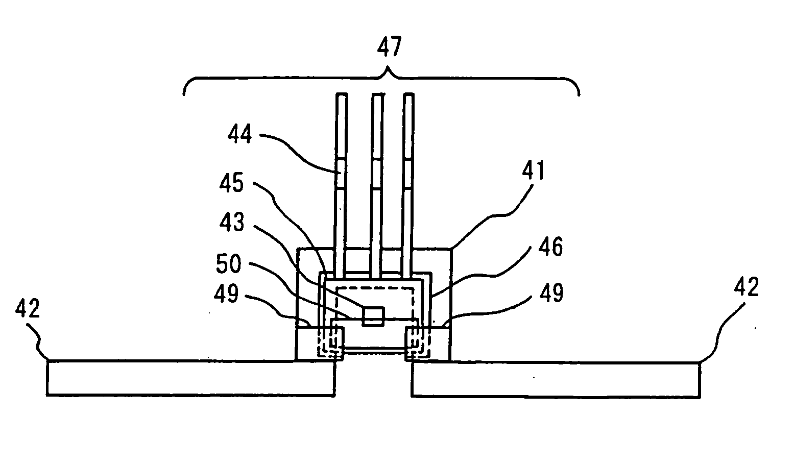
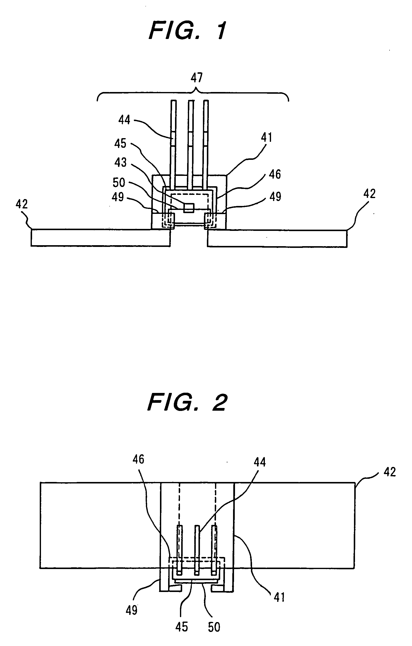
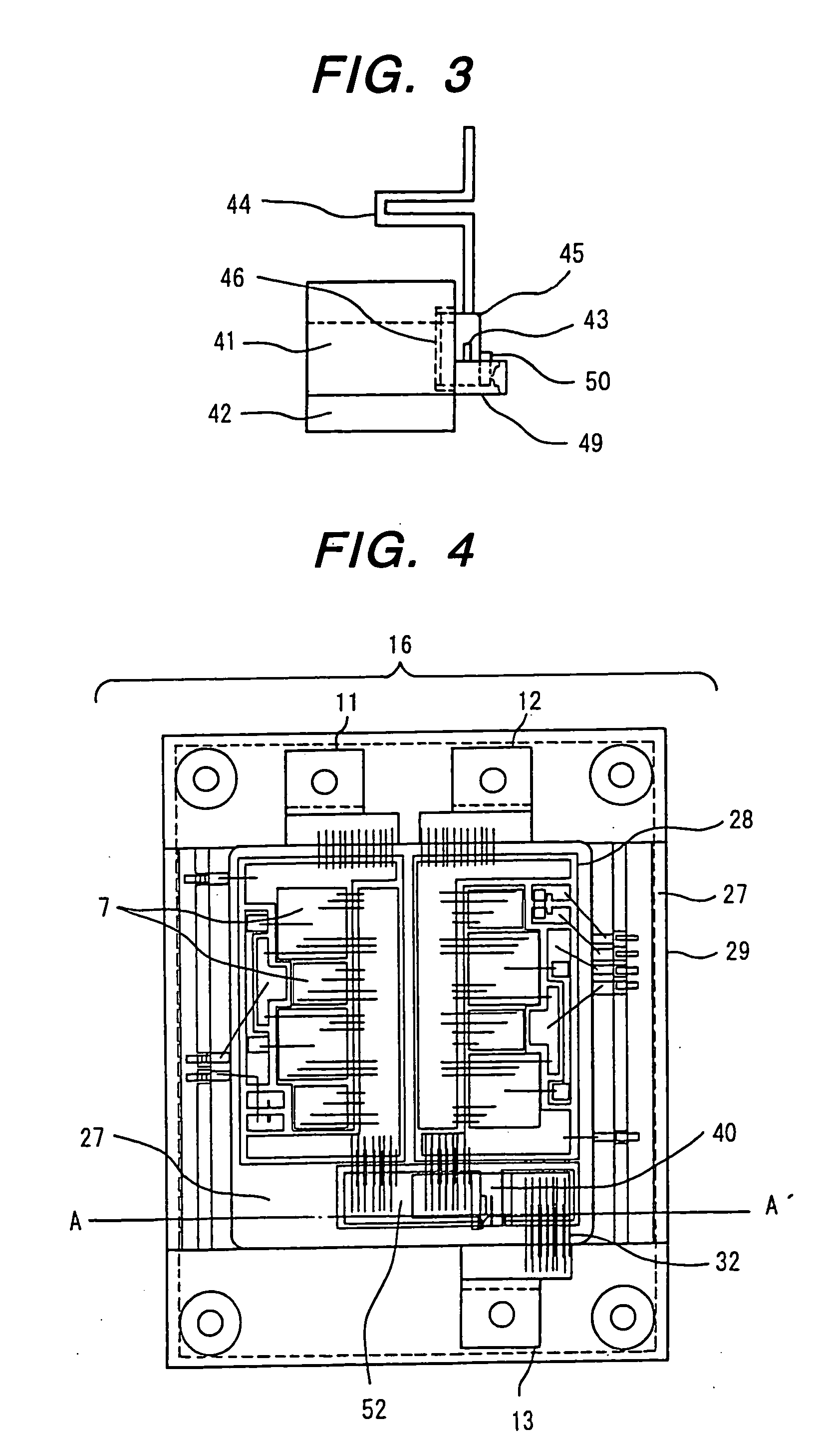
[0248] A second embodiment of the present invention will be explained with reference to FIGS. 10 through 12. FIGS. 10 through 12 show the configuration of a current detector incorporated into a power converter of this embodiment. This embodiment is an altered example of the first embodiment. In this embodiment, a magnetic detecting semiconductor element 43 is fixed onto the printed wiring board 53 which is configured such that a plurality of laminated wiring sheets 54, each of which consists of a resin insulation layer and a laminated copper foil, are laminated; and a magnetic detecting unit 47 is provided in which the magnetic detecting semiconductor element 43 has electrical connections with the laminated wiring sheets 54 via aluminum wires, and connection terminals 44 have electrical connections with the laminated wiring sheets 54. The magnetic detecting semiconductor element 43 is covered with molded resin 45.
[0249] For example, the laminated wiring sheets 54 are disposed together with a wide shield electrode which is wired on the same wiring layer and allows most of the laminated wiring sheets 54 to overlap in a different wiring layer. Or, some of the laminated wiring sheets 54 are arranged on different wiring layers, and the laminated wiring sheets 54 are also disposed such that they overlap with the entire area. In the latter case, electronic parts, such as a chip capacitor 56, can be installed between the laminated wiring sheets 54.
[0250] A depression 46 is provided in the detection conductor 41 in the same manner as the first embodiment. A part of the magnetic detecting unit 47 is contained in the depression 46 so that connection terminals 44 extend in the same direction as shown in the first embodiment.
[0251] Two fixing jigs abut on a printed wiring board 53, which is not opposite to the depression 46 in the magnetic detecting unit 47, with an adhesion layer 50 interposed. The fixing jig is an arm-like protruding portion 49 which is created such that the detection conductor 41 protrudes into the printed wiring board 53, which is not opposite to the depression 46 in the magnetic detecting unit 47, so that the fixing jigs surround (embrace) the part of the printed wiring board 53. The adhesion layer 50 is elastic enough to press the magnetic detecting unit 47 or the adhesion layer 50 becomes hard and adhesive by being processed by a prescribed procedure, thereby bonding together the printed wiring board 0.53 and the protruding portion 49. The other configuration is the same as the first embodiment, and therefore, a specific description will be omitted.
[0252] According to this embodiment, the same effect as the first embodiment can be obtained, and it is also possible to flexibly change the shape of the connection terminals 44 which have electrical connections with the laminated wiring sheets 54 of the printed wiring board 53. Therefore, according to this embodiment, it is possible to increase the degree of flexibility of the connection system with the control board 55 of the control unit 26, and connection by means of a connector is also easily carried out.
[0253] Furthermore, according to this embodiment, the laminated wiring sheets 54 are disposed together with a wide shield electrode which is wired on the same wiring layer and allows most of the laminated wiring sheets 54 to overlap in a different wiring layer; or, some of the laminated wiring sheets 54 are arranged on different wiring layers, and the laminated wiring sheets 54 are also disposed such that they overlap with the entire area. Accordingly, it is possible to reduce magnetic flux (noise) which interlinks with the electrical annular wire connection created by circuit wiring of the control board 55, and therefore, it is possible to dispose noise control parts, such as a chip capacitor 56, in proximity to the magnetic detecting semiconductor element 43. As a result, according to this embodiment, the accuracy of the current detector 40 can be increased.
Example
[0254] A third embodiment of the present invention will be explained with reference to FIGS. 13 through 15. FIGS. 13 through 15 show the configuration of a current detector incorporated into a power converter of this embodiment. This embodiment is an altered example of the first embodiment. In this embodiment, a magnetic detecting unit 47 configured in the same manner as the first embodiment is provided, and a part of the magnetic detecting unit 47 is contained in the depression 46 of the detection conductor 41, which is provided in the same manner as the first embodiment, so that connection terminals 44 extend in the same direction as shown in the first embodiment.
[0255] The bottom portion of the nearly letter-U shaped resin formed body 57 having a protruding/recessed portion 58 is inserted into the cavity of the detection conductor 41 from one side of the detection conductor 41 which is the opposite side of the magnetic detecting unit 47 side, and is engaged with the detection conductor 41 so that the resin formed body 57 embraces the portion which is parallel to the current detection electrode 42 of the detection conductor 41. A claw 59 is formed at the tip of the bottom portion of the resin formed body 57. The claw-like protrusion of the claw 59 abuts on the molded resin 45, which is not opposite to the depression 46 in the magnetic detecting unit 47, with an adhesion layer 50 interposed, thereby securing the magnetic detecting unit 47. A concave portion into which connection terminals 44 are allowed to fit is created at the tip of the top portion of the resin formed body 57. The connection terminals 44 are fit into the concave portion located at the tip of the top portion of the resin formed body 57, and thus the connection terminals 44 are supported. The resin formed body 57 functions as a fixing jig for the magnetic detecting unit 47. The other configuration is the same as the first embodiment, and therefore, a specific description will be omitted.
[0256] In the current detector 40 configured as stated above, by means of the soldering process in which for several minutes at a high temperature a power controlling semiconductor element 7 is soldered, a detection conductor 41 is soldered onto the electrode 52 of the ceramic substrate 28. After that, the resin formed body 57 is inserted into the detection conductor 41 by using the protruding/recessed portion 58 formed on the resin formed body 57, thereby enabling the resin formed body 57 to engage with the detection conductor 41. Then, the magnetic detecting unit 47 is inserted into the depression 46 created in the detection conductor 41, and the claw-like protrusion of the claw 59 of the resin formed body 57 abuts on the molded resin 45, which is not opposite to the depression 46 in the magnetic detecting unit 47, with an adhesion layer 50 interposed, thereby securing the magnetic detecting unit 47 onto the detection conductor 41.
[0257] According to this embodiment, the same effect as the first embodiment can be obtained, and by integrating a resin formed body 57, which is blended with magnetic powder, and a detection conductor 41 into a magnetic circuit on the resin formed body 57, it is possible to improve the amount of magnetic flux inputted into the magnetic detecting unit 47. Therefore, according to this embodiment, detection sensitivity of the current detector 40 can be increased.
PUM


Description & Claims & Application Information
We can also present the details of the Description, Claims and Application information to help users get a comprehensive understanding of the technical details of the patent, such as background art, summary of invention, brief description of drawings, description of embodiments, and other original content. On the other hand, users can also determine the specific scope of protection of the technology through the list of claims; as well as understand the changes in the life cycle of the technology with the presentation of the patent timeline. Login to view more.
Similar technology patents
Bayonet vehicle image identification method based on image features
Owner:SUN YAT SEN UNIV +1
Metrology Method and Apparatus, Substrate, Lithographic System and Device Manufacturing Method
Owner:ASML NETHERLANDS BV
Gesture recognition method and gesture recognition device
Owner:SHENZHEN ORBBEC CO LTD
TR309 - portable otoscope video viewer
Owner:RICH TONY C +1
Classification and recommendation of technical efficacy words
- improve accuracy
Golf club head with adjustable vibration-absorbing capacity
Owner:FUSHENG IND CO LTD
Direct fabrication of aligners for arch expansion
Owner:ALIGN TECH
Stent delivery system with securement and deployment accuracy
Owner:BOSTON SCI SCIMED INC
Method and apparatus for image-based eye tracking for retinal diagnostic or surgery device
Owner:SENSOMOTORIC INSTR FUR INNOVATIVE SENSORIK MBH D B A SENSOMOTORIC INSTR +1
Method for improving an HS-DSCH transport format allocation
Owner:NOKIA SOLUTIONS & NETWORKS OY