Display device and driving method thereof

a technology of a display device and a driving method, applied in the direction of static indicating devices, instruments, etc., can solve the problems of screen burn and difficulty in obtaining the same luminance, and achieve the effect of improving reliability and reliability

Inactive Publication Date: 2005-07-28
SEMICON ENERGY LAB CO LTD
View PDF49 Cites 57 Cited by
  • Summary
  • Abstract
  • Description
  • Claims
  • Application Information

AI Technical Summary

Benefits of technology

[0011] Preferably, by fixing the gate potential of the driving transistor, it can operate without the gate-source voltage Vgs thereof being changed by parasitic capacitance or wiring capacitance. As a result, display unevenness due to the variations in the gate-source voltage Vgs of the driving transistor can be suppressed.
[0013] The driving transistor can operate in the saturation region and the linear region while the switching transistor, the current controlling transistor and the erasing transistor operate in the linear region. When transistors operate in the linear region, drive voltage thereof can be low, therefore, low power consumption of a display device can be achieved.
[0018] According to the invention, a circuitry and a driving method thereof in which a reverse voltage is applied to a light emitting element in order to control the degradation thereof and improve reliability, can be provided for a display device comprising a pixel circuit. Further, a reverse voltage can be applied without an anode line and a signal line being short-circuited, namely without the anode line and a power source line of a signal line driver circuit being short-circuited. As a result, a long-life electronic device having a display device can be achieved.
[0019] Accordingly, a circuitry and a driving method thereof in which a reverse voltage is applied to a light emitting element in order to control the degradation thereof and improve reliability can be provided for a display device comprising a pixel circuit.

Problems solved by technology

In addition, degradation of the light emitting element with the passage of time makes it difficult to obtain the same luminance even with a certain current supplied.
Further, variations of the degradation level of each light emitting element cause a screen burn.

Method used


Image

  • Display device and driving method thereof
  • Display device and driving method thereof
  • Display device and driving method thereof

Examples


embodiment mode 1

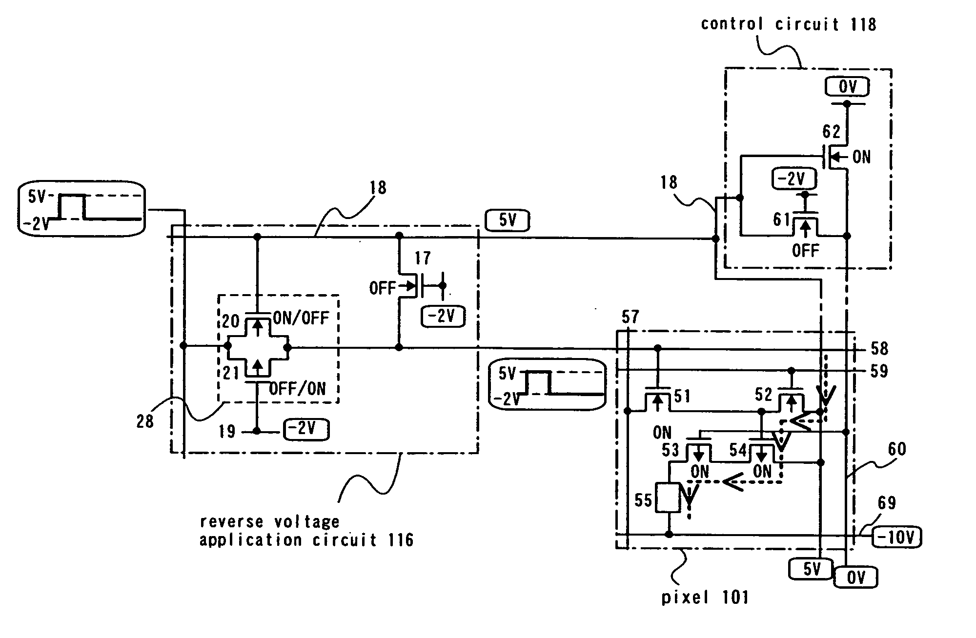
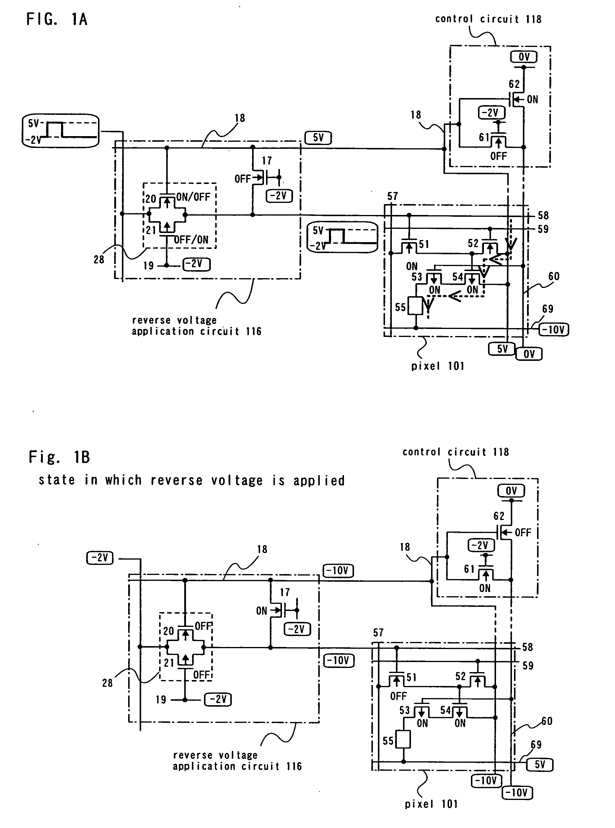
[0037] In this embodiment mode, description is made on an illustrative example of a pixel circuit comprising at least a switching transistor, an erasing transistor, a driving transistor and a current controlling transistor, wherein a reverse voltage application circuit comprising an analog switch is provided.

[0038]FIG. 1A illustrates the state in which a forward voltage (voltage in the direction by which a light emitting element emits light) is applied, and a light emitting element emits light accordingly. A reverse voltage application circuit 116 comprises an analog switch 28 having an N-channel transistor 20 and a P-channel transistor 21. The gate electrode of the N-channel transistor 20 is connected to an anode line 18, and the anode line 18 is fixed at 5 V in this embodiment mode. The gate electrode of the P-channel transistor 21 is connected to a power source line at a fixed potential or a cathode line 69. In this embodiment mode, it is connected to a first power source line 1...

embodiment mode 2

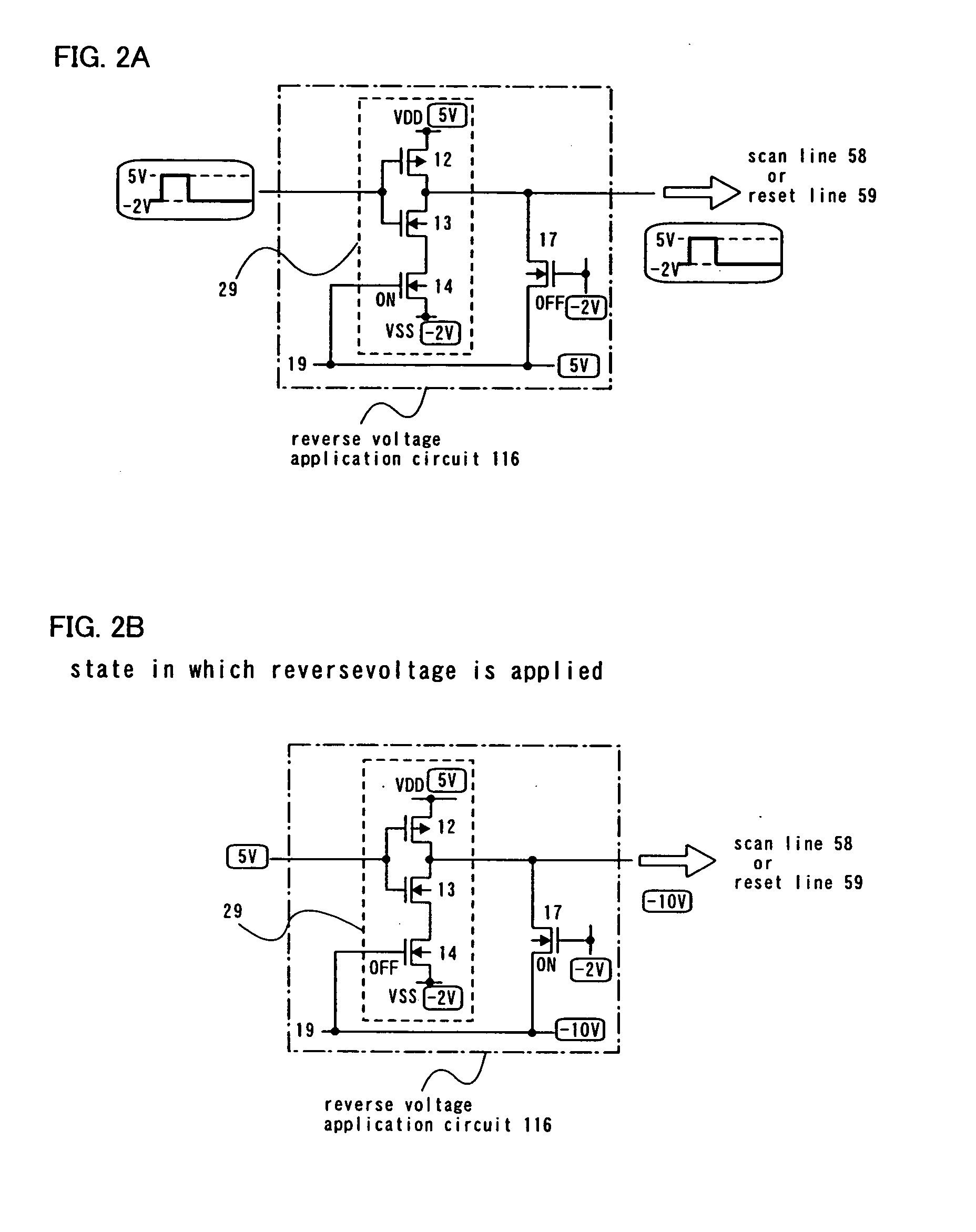
[0057] In this embodiment mode, description is made on an illustrative example in which the invention is applied to a reverse voltage application circuit which comprises a clocked inverter.

[0058]FIG. 2A illustrates the state in which a forward voltage is applied. The reverse voltage application circuit 116 shown in FIG. 2A comprises a clocked inverter 29 having a P-channel transistor 12 and N-channel transistors 13 and 14 connected in series. Note that the clocked inverter may further have another P-channel transistor. The gate electrode of the P-channel transistor 12 and the gate electrode of the N-channel transistor 13 have the same potentials, namely they are connected. The first electrode of the P-channel transistor 12 is connected to a power source line at a fixed potential, for example, to a VDD (high potential power source line) fixed at 5 V. The first electrode of the N-channel transistor 14 is connected to a power source line at a fixed potential, for example, to a VSS (lo...

embodiment mode 3

[0072] In this embodiment mode, description is made on a scan line driver circuit and a signal line driver circuit comprising a reverse voltage application circuit, and a display device including them.

[0073]FIG. 5A illustrates a configuration of a scan line driver circuit which comprises a shift register 114, a buffer circuit 115 and a reverse voltage application circuit portion 150 which includes the reverse voltage application circuit 116.

[0074] The reverse voltage application circuit portion 150 comprises a plurality of the reverse voltage application circuits 116 and the reverse voltage application transistors 17 each of which is connected to the scan line or the reset line as shown in FIGS. 1A to 2B. The reverse voltage application circuit 116 comprises the analog switch 28 or the clocked inverter 29.

[0075] In the case of providing the reverse voltage application circuit portion 150 in the scan line driver circuit, a potential of the anode line, and a fixed potential of the ...


PUM


Abstract

A circuitry and a driving method thereof in which a reverse voltage is applied to a light emitting element to control the degradation thereof and improve reliability for a display device comprising a pixel circuit. A first power source line is connected to a signal line through a switching transistor and erasing transistor, and a current controlling transistor and driving transistor are connected in series between the first power source line and a light emitting element. An analog switch including first and second transistors whose gate electrodes are connected to the first and second power source lines respectively is provided. Further, a bias transistor whose gate electrode is connected to a third power source line, one of source and drain electrodes thereof is connected to the first power source line, and the other is connected to an output terminal of the analog switch and a scan line is provided.

Description

BACKGROUND OF THE INVENTION [0001] 1. Field of the Invention [0002] The present invention relates to a display device having light emitting elements and a driving method thereof. [0003] 2. Description of the Related Art [0004] In recent years, display devices formed by using light emitting elements (self-luminous light emitting elements) are actively researched and developed. Such display devices are widely used as a display screen of a mobile phone, a monitor of a personal computer and the like by utilizing the advantages of high image quality, thin shape, lightweight and the like. In particular, since such display devices have features of high response speed, low voltage and low power consumption drive and the like that are suitable for displaying moving images, it is expected to have a wide scope of application including those for next-generation mobile phones or portable information terminals (PDAs). [0005] Luminance of a light emitting element decays with the passage of time. F...

Claims


Application Information

Patent Timeline
Patent Type & Authority Applications(United States)
IPC IPC(8): G09G3/30G09G3/32
CPCG09G3/3233G09G3/3258G09G3/3266G09G3/3275G09G2320/043G09G2310/0251G09G2310/0254G09G2310/0256G09G2300/0842
Inventor OSAME, MITSUAKIANZAI, AYAYAMAZAKI, YUFUKUMOTO, RYOTA
Owner SEMICON ENERGY LAB CO LTD
Why Eureka
Try Eureka