Image display apparatus and method of forming

a technology of liquid crystal display and display device, which is applied in the direction of static indicating device, instruments, non-linear optics, etc., can solve the problems of non-uniform brightness, difficult to achieve a uniform vsub>feedthrough /sub>of a tft, and difficulty in achieving uniform brightness of the display

Inactive Publication Date: 2005-07-28
INNOLUX CORP
View PDF7 Cites 11 Cited by
  • Summary
  • Abstract
  • Description
  • Claims
  • Application Information

AI Technical Summary

Benefits of technology

[0022] The present invention resolves the above problems and thus is able to provide an image display apparatus capable of suppressing a voltage change that exists at a pixel electrode, ΔVpixel, in a pixel circuit due to voltage signals transmitted from a switching component in the pixel circuit as well as from neighboring pixel circuits.

Problems solved by technology

The voltage at the pixel electrode 30 changes with a corresponding change in the display brightness which leads to non-uniform brightness.
It is difficult to achieve a uniform Vfeedthrough of a TFT that can accurately respond to a continuous change in the voltage amplitude Vscan.
A border region in-between the pixel circuits that has different parasitic capacitances can make the brightness of the display non-uniform if the parasitic capacitance Cgs is not continuously changed when transitioning between neighboring pixels located along a scan line.
However, due to present processing constraints, the size of the overlapping region between the source and the gate region is limited to about 0.9 μm.
Because of these limitations, It is difficult to manufacture a TFT having pre-determined Cgs capacitances that can compensate for pulse voltage input Vscan voltage changes and Vfeedthrough changes for each pixel in a pixel matrix located on a TFT matrix display.
Continuous adjustment of the Cgs by changing the structure of each TFT within each pixel to increase the overlapping region beyond a width range of 0.25 to 0.5 μm is not feasible.
Thus, it is not possible to rely on the design and process definition of a TFT to enable a constant Vfeedthrough of each of a plurality pixel circuits located at varying distances from the scan line driver circuit.
Moreover, the problem of parasitic capacitance produced in each pixel circuit exists beyond the scanning lines.
Accordingly, it is difficult to compensate feed-through voltages for all pixels by adjusting the voltage of the common counter electrode.
Therefore, it is hard to provide a TFT-LCD without a flicker.

Method used


Image

  • Image display apparatus and method of forming
  • Image display apparatus and method of forming
  • Image display apparatus and method of forming

Examples


Embodiment Construction

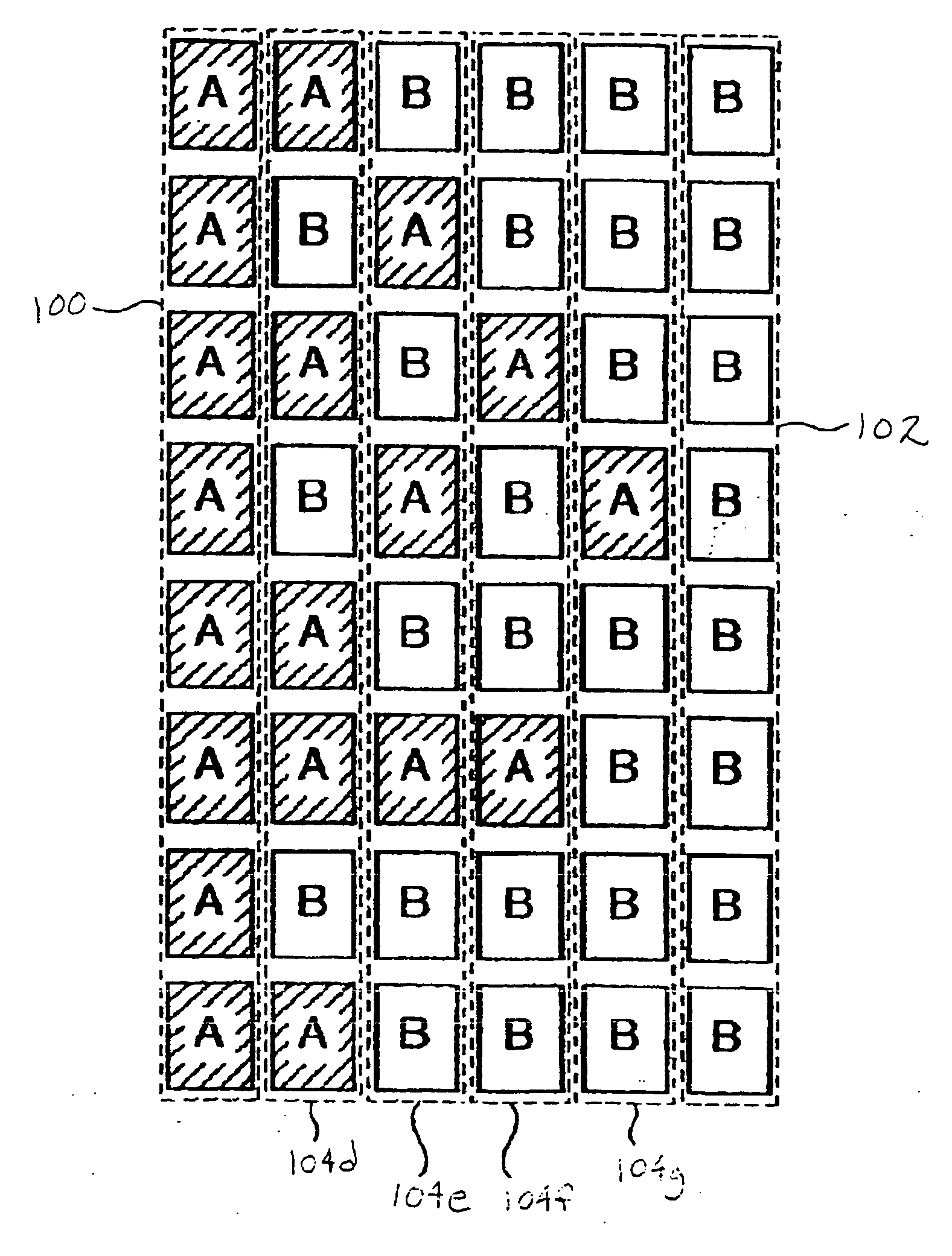
[0044] Exemplary embodiments of an image display device and a liquid crystal display apparatus according to the present invention are explained below with reference to the drawings. In the following embodiments, when there is a plurality of parts of the same configuration, one of these parts is explained as a representative when necessary.

[0045] When the same part is explained using a plurality of drawings, a reference symbol shown in one drawing will also be used in the rest of the drawings. Identification characters a, b, c, etc. are assigned to reference symbols when necessary. When there are a plurality of the same parts like “scan line driver 72a, and 72b”, these parts are collectively called a “scan line driver 72” when necessary.

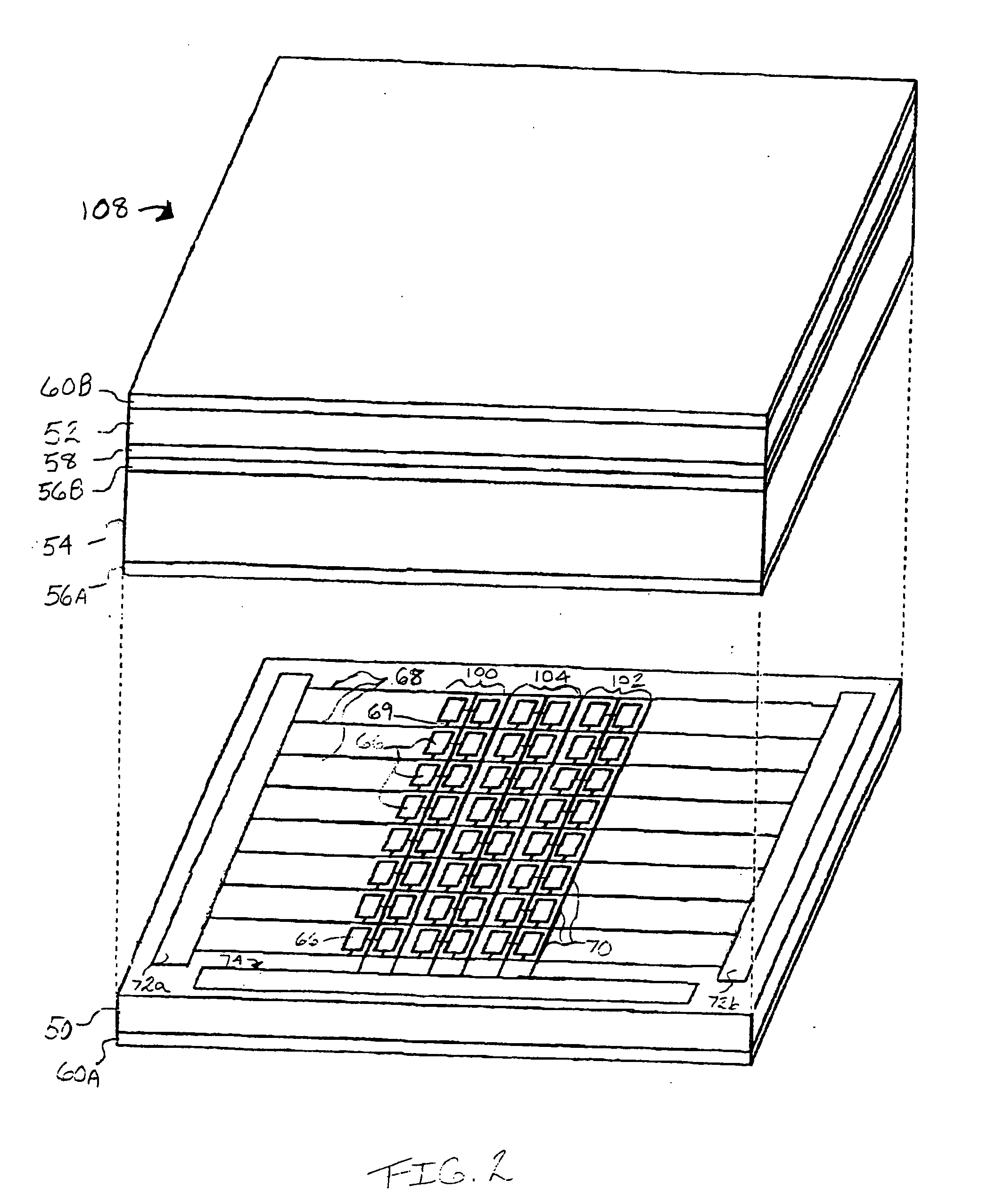
[0046]FIG. 2 shows a perspective, analytical view of a complete structure of an image display apparatus in a preferred embodiment of the present invention. The image display apparatus is constructed by a configuration having a plurality TFT-LCD disp...


PUM

PropertyMeasurementUnit
widthaaaaaaaaaa
sizeaaaaaaaaaa
widthaaaaaaaaaa

Abstract

An image display apparatus and method that provides a flicker-proof thin-film-transistor liquid-crystal-display (TFT-LCD) is provided. The TFT-LCD has a first pixel circuit group having a plurality of first pixel circuits each having a first capacitance; a second pixel circuit group having a plurality of second pixel circuits each having a second capacitance; and a third pixel circuit group having a plurality of the first pixel circuits and the second pixel circuits arranged in accordance with a weighted average of m number of first pixel circuits and n number of second pixel circuits. The m and n first and second pixel circuits form an average third capacitance greater than the first capacitance of the plurality of first pixel circuits but less than the second capacitance of the plurality of second pixel circuits, wherein m and n are positive integers. The pixel circuit groups are formed on a matrix substrate.

Description

CROSS-REFERENCE TO RELATED APPLICATIONS [0001] This is a cross-related Patent Application under 35 USC Section 119 (a) that claims a priority date of Nov. 28, 2003 from co-pending Japanese Application No. 2003-400090, filed on Nov. 28, 2003, the disclosure of which is incorporated by reference. TECHNICAL FIELD [0002] The present invention relates in general to an image display apparatus that provides thin-film-transistor liquid-crystal-display (TFT-LCD). In particular, the present invention relates to a flicker-proof thin-film-transistor liquid-crystal-display and method of forming. BACKGROUND OF THE INVENTION [0003] The structure of a conventional thin film transistor liquid crystal display (TFT-LCD) is comprised essentially of LCD cells comprising a pair of electrode substrates filled with liquid crystal molecules. Polarizers are adhered to the sides of the electrode substrates. Signal lines and scanning lines are formed perpendicularly with each other forming a matrix on one of t...

Claims


Application Information

Patent Timeline
Patent Type & Authority Applications(United States)
IPC IPC(8): G02F1/133G02F1/1343G02F1/1362G02F1/1368G09G3/20G09G3/36H01L51/50H05B33/14
CPCG02F1/136286G09G3/3648G09G2320/0247G09G2320/0214G09G2300/0852
Inventor TAKASUGI, SHINJINAGAYAMA, KAZUYOSHIIKEZAKI, MITSURI
Owner INNOLUX CORP
Why Eureka
Try Eureka