Liquid crystal display device

a display device and liquid crystal technology, applied in non-linear optics, instruments, optics, etc., can solve the problems of reducing the response time of grayscale display, affecting the uniformity of display, and affecting the quality of display, so as to reduce the roughness of display recognized when grayscale display is viewed in a slanting direction, the effect of improving uniformity and improving display

Inactive Publication Date: 2005-07-28
SHARP KK
View PDF25 Cites 8 Cited by
  • Summary
  • Abstract
  • Description
  • Claims
  • Application Information

AI Technical Summary

Benefits of technology

[0044] In the liquid crystal display device in the first aspect of the present invention, the directions in which liquid crystal molecules tilt during voltage application (during generation of an electric field) are defined with the slope face effect of the wall structure formed on the surface of the first substrate facing the liquid crystal layer in the shading region, so that an axisymmetrically aligned domain is formed. At least either one of an arbitrary row and an arbitrary column of the plurality of pixels has first pixels each having the first electrode to which a voltage of positive polarity with respect to the potential at the second electrode as the reference potential is supplied, and second pixels each having the first electrode to which a voltage of negative polarity is supplied, arranged alternately, in a given vertical scanning period. Accordingly, a steeply inclined electric field is generated between the first pixel and the second pixel, and with this inclined electric field, the axisymmetrically aligned domain is stabilized. The inclined electric field generated by applying voltages of opposite polarity to the first electrodes of pixels adjacent to each other acts, together with the alignment regulating force of the side slopes of the wall structure provided between the adjacent pixels and the effect of distortion of the electric field due to the existence of the wall structure, to stabilize the alignment of the axisymmetric domain. The alignment regulating force of the side slopes of the wall structure acts irrespective of generation of the electric field, and the electric field is distorted with the existence of the wall structure. Therefore, the axisymmetric alignment can be stabilized even in a grayscale display state.
[0056] When the present invention is applied to a transflective LCD device, a transparent dielectric layer may be placed on the second substrate for control of the thickness of the liquid crystal layer. With this construction, an invalid region that does not contribute to display during transmission display can be reduced compared with the conventional transflective LCD device in which the transmission region and the reflection region are differentiated from each other by forming a step on the first substrate, and thus the brightness in transmission display can be improved. The diffuse reflection plate for improving the brightness in the reflection region may be provided on the first substrate in the reflection region. Otherwise, a light scattering layer (light diffuse layer) may be formed on the transparent dielectric layer on the second substrate. This can eliminate the necessity of forming projections and depressions on the surface of the reflection electrode.

Problems solved by technology

However, in the device described in Literature 1, it is difficult to generate an inclined electric field over the entire region of each pixel.
Therefore, each pixel has a region in which liquid crystal molecules delay in response to a voltage, and this causes a problem of occurrence of an afterimage phenomenon.
According to examinations conducted by the inventors of the present invention, however, to obtain sufficient alignment regulating force, it is necessary to form an alignment control structure made of projections regularly placed inside each pixel, and this complicates the fabrication process.
This technology therefore has the same problems as those described above.
Also, sufficient alignment regulating force will not be exerted in a grayscale display state having a low electric field.
This causes a problem of easily generating disclination (alignment defect) in the corner portions of each pixel.

Method used


Image

  • Liquid crystal display device
  • Liquid crystal display device
  • Liquid crystal display device

Examples


embodiment 1

[0069] Hereinafter, LCD devices of Embodiment 1 of the present invention will be described concretely with reference to FIGS. 1A / B to 4, 5A and 6 to 11.

(Transmissive LCD Device)

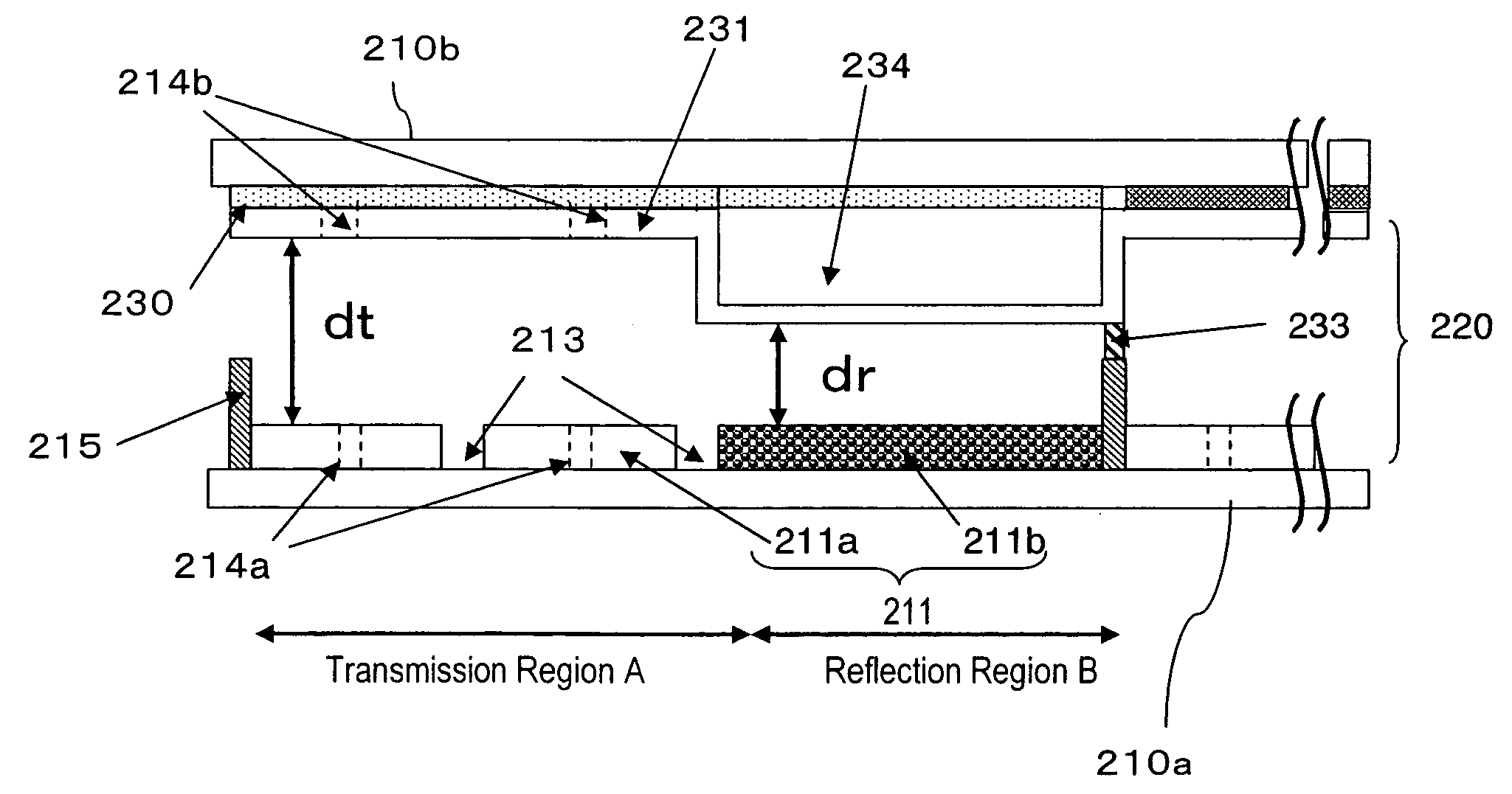
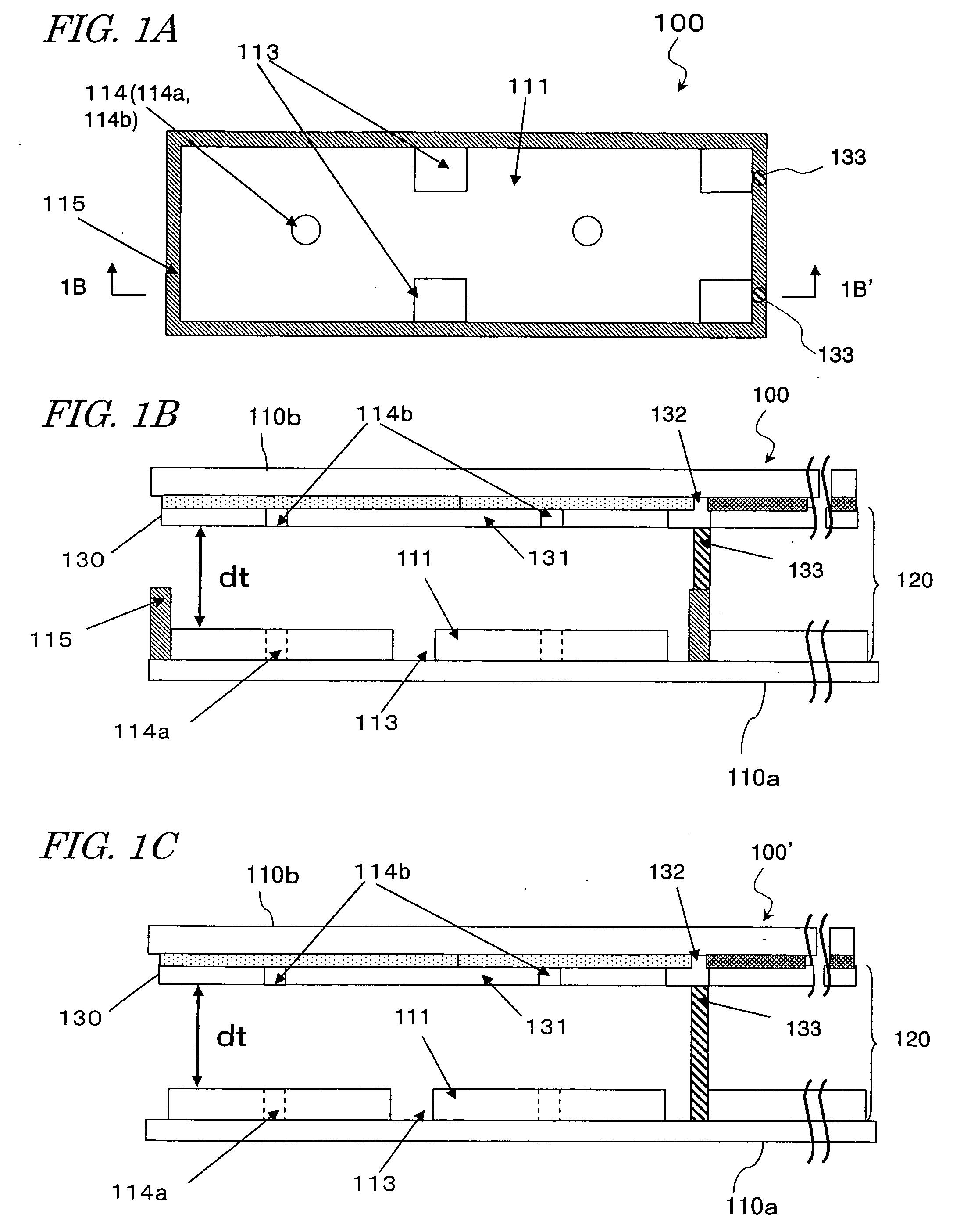
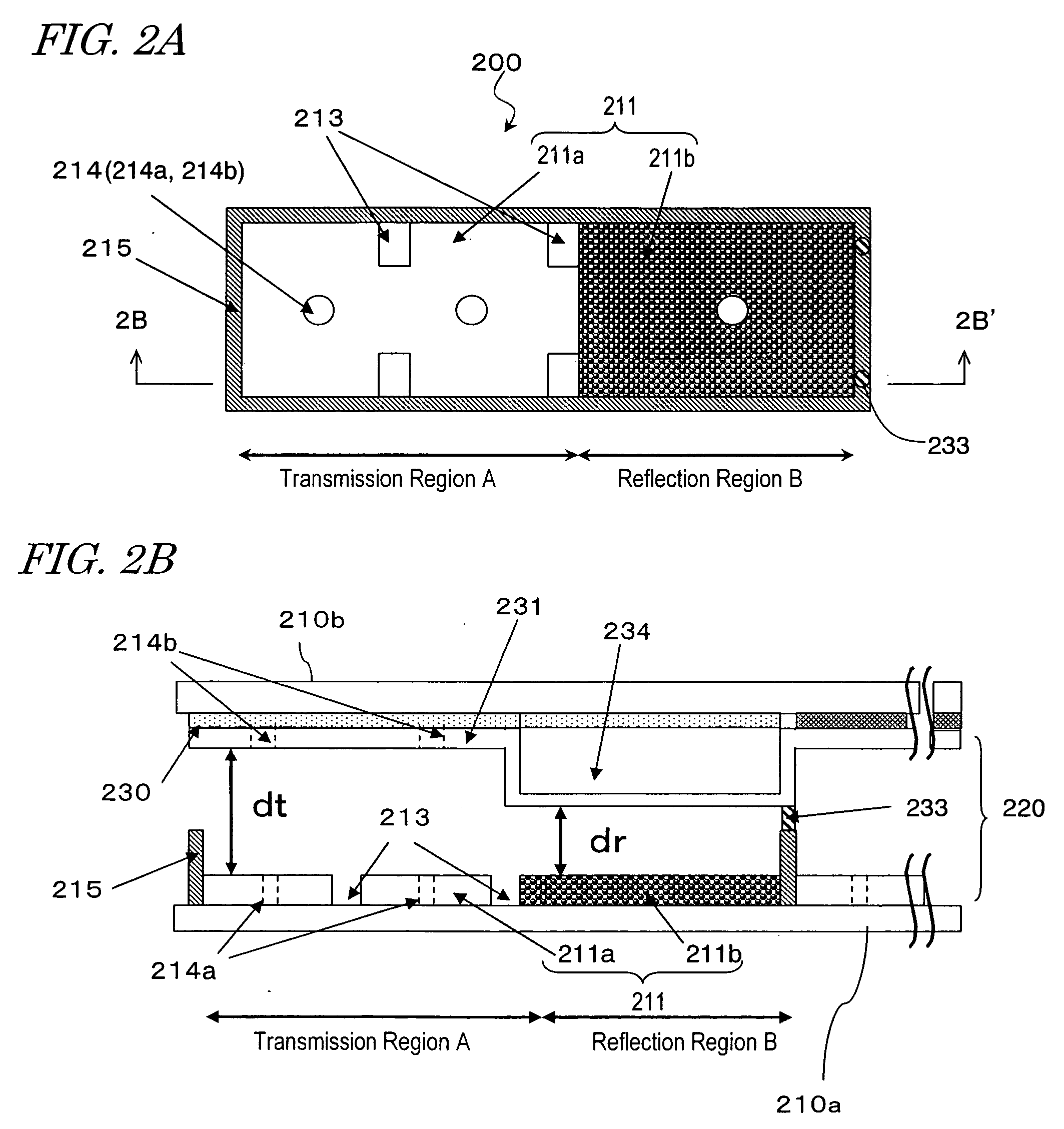
[0070] A transmissive LCD device 100 of Embodiment 1 of the present invention will be described with reference to FIGS. 1A and 1B. FIGS. 1A and 1B diagrammatically show one pixel of the transmissive LCD device 100, in which FIG. 1A is a plan view and FIG. 1B is a cross-sectional view taken along line 1B-1B′ in FIG. 1A.

[0071] Hereinafter, described will be the case that one pixel is divided into two parts (N=2). The number of parts into which one pixel is divided (=N) can also be three or more depending on the pixel pitch. In any case, the number of openings (=n) each to be positioned roughly in the center of a divided region on a second substrate is preferably the same as the number of divided parts (=N). The effective aperture ratio tends to decrease with increase of the number of divided parts (=N). The...

embodiment 2

[0159] Hereinafter, LCD devices of Embodiment 2 of the present invention will be described concretely with reference to FIGS. 1A / B / C to 4, 5B and 6 to 11. The LCD devices of Embodiment 2 are different from the LCD devices of Embodiment 1 in that only the dot inversion drive is adopted and that the wall structure can be omitted.

(Transmissive LCD Device)

[0160] A transmissive LCD device 100 of Embodiment 2 of the present invention will be described with reference to FIGS. 1A and 1B. FIGS. 1A and 1B diagrammatically show one pixel of the transmissive LCD device 100, in which FIG. 1A is a plan view and FIG. 1B is a cross-sectional view taken along line 1B-1B′ in FIG. 1A. FIG. 1C is a cross-sectional view diagrammatically showing one pixel of another transmissive LCD device 100′.

[0161] Hereinafter, described will be the case that one pixel is divided into two parts (N=2). The number of parts into which one pixel is divided (=N) can also be three or more depending on the pixel pitch. I...


PUM

PropertyMeasurementUnit
thicknessaaaaaaaaaa
drive voltageaaaaaaaaaa
widthaaaaaaaaaa

Abstract

The liquid crystal display device includes a first substrate, a second substrate opposed to the first substrate, and a vertically aligned liquid crystal layer interposed between the first and second substrates, and has a plurality of pixels arranged in a matrix having rows and columns. Each pixel includes a first electrode formed on the first substrate, a second electrode formed on the second substrate, and the liquid crystal layer interposed between the first and second electrodes. The first substrate has a shading region in gaps between the plurality of pixels, and a wall structure is placed regularly on the surface of the first substrate facing the liquid crystal layer in the shading region. The first and second electrodes have at least one opening formed at a predetermined position in the pixel. At least an arbitrary row or column of pixels is composed of first pixels each having the first electrode to which a voltage of positive polarity with respect to the potential at the second electrode as the reference potential is supplied and second pixels each having the first electrode to which a voltage of negative polarity is supplied, arranged alternately, in a given vertical scanning period. At least one liquid crystal domain having axisymmetric alignment is formed when at least a predetermined voltage is applied across the liquid crystal layer, and the center axis of the axisymmetric alignment of the at least one liquid crystal domain is formed in or near the at least one opening.

Description

BACKGROUND OF THE INVENTION [0001] The present invention relates to a liquid crystal display device and a fabrication method for the same, and more particularly, to a liquid crystal display device suitably used for portable information terminals (for example, PDAs), mobile phones, car-mounted liquid crystal displays, digital cameras, PCs, amusement equipment, TVs and the like. [0002] The information infrastructure is advancing day to day, and equipment such as mobile phones, PDAs, digital cameras, video cameras and car navigators has penetrated deeply into people's lives. Liquid crystal display (LCD) devices have been adopted in most of such equipment. With increase of the information amount handled with the main bodies of the equipment, LCD devices are requested to display a larger amount of information, and are demanded by the market for higher contrast, a wider viewing angle, higher brightness, multiple colors and higher definition. [0003] A vertical alignment mode using a vertic...

Claims


Application Information

Patent Timeline
Patent Type & Authority Applications(United States)
IPC IPC(8): G02F1/1337G02F1/1333G02F1/1335G02F1/1339G02F1/1343G02F1/136G02F1/139
CPCG02F1/133555G02F1/1393G02F1/13394G02F1/133707G02F1/1335G02F1/1337
Inventor KUME, YASUHIROTAMAI, KAZUHIKONAGAE, NOBUKAZUONISHI, NORIAKI
Owner SHARP KK
Why Eureka
Try Eureka