Semiconductor device having radiation structure

a radiation structure and semiconductor technology, applied in the details of semiconductor/solid-state devices, semiconductor devices, electrical apparatus, etc., can solve the problems of increasing the chip size, limited disposal of different semiconductor chips in one device, and increasing the stress concentration of the first conductive member, so as to improve the radiation property and electrical conductivity of the semiconductor device, and prevent the occurrence of cracks.

Inactive Publication Date: 2005-08-04
DENSO CORP
View PDF42 Cites 28 Cited by
  • Summary
  • Abstract
  • Description
  • Claims
  • Application Information

AI Technical Summary

Benefits of technology

[0012] The present invention has been made in view of the above problem. An object of the present invention is to improve a radiation property and an electrical conductivity of a semiconductor device including radiation members that are thermally and electrically connected to both surfaces of a semiconductor chip therein. Another object of the present invention is to provide a semiconductor device easily accommodating several different semiconductor chips therein.
[0013] For example, according to one aspect of the present invention, in a semiconductor device in which a semiconductor chip is thermally and electrically connected to first and second radiation members therebetween, the first and second radiation members are made of a metallic material that is superior to tungsten and molybdenum in at least one of an electrical conductivity and a thermal conductivity. Accordingly, the radiation property and the electrical conductivity of the semiconductor device can be improved.
[0016] According to still another aspect of the present invention, in a semiconductor device in which a semiconductor chip is disposed between a first conductive member and a second conductive member, the first conductive member is further bonded to a third conductive member at an opposite side of the semiconductor chip so that a bonding area between the first conductive member and the third conductive member is smaller than that between the first conductive member and the semiconductor chip. Accordingly, stress concentration on the first conductive member can be suppressed to prevent occurrence of cracks. This results in improved radiation property and electrical conductivity of the semiconductor device.

Problems solved by technology

Thus, in the present circumstances involving an increased requirement for flowing a large current in the semiconductor chip, using W or Mo as a member that serves as a radiation member and an electrode simultaneously causes many problems.
However, there are many technological problems to increase the chip size, and it is easier to manufacture plural smaller chips and accommodate them into one package.
However, as shown in FIG. 1A, because the radiation member J2 has a simple rectangular shape, and is provided at the center of the device, disposal of different semiconductor chips in one device is limited.
That is, when the semiconductor chips are different from one another in, for example, thickness, it is difficult for the one emitter electrode having a simple shape to be connected to all of the different semiconductor chips.

Method used


Image

  • Semiconductor device having radiation structure
  • Semiconductor device having radiation structure
  • Semiconductor device having radiation structure

Examples


first embodiment

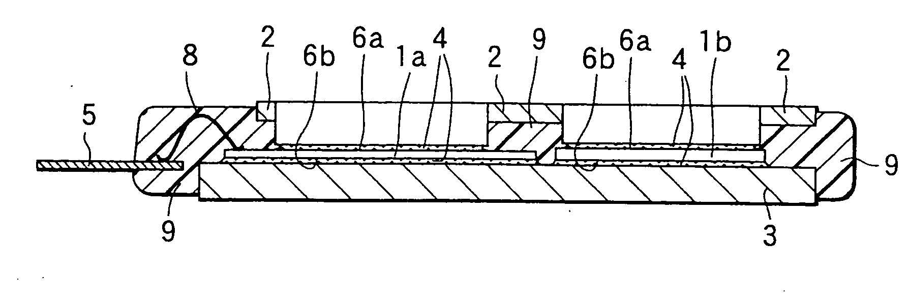
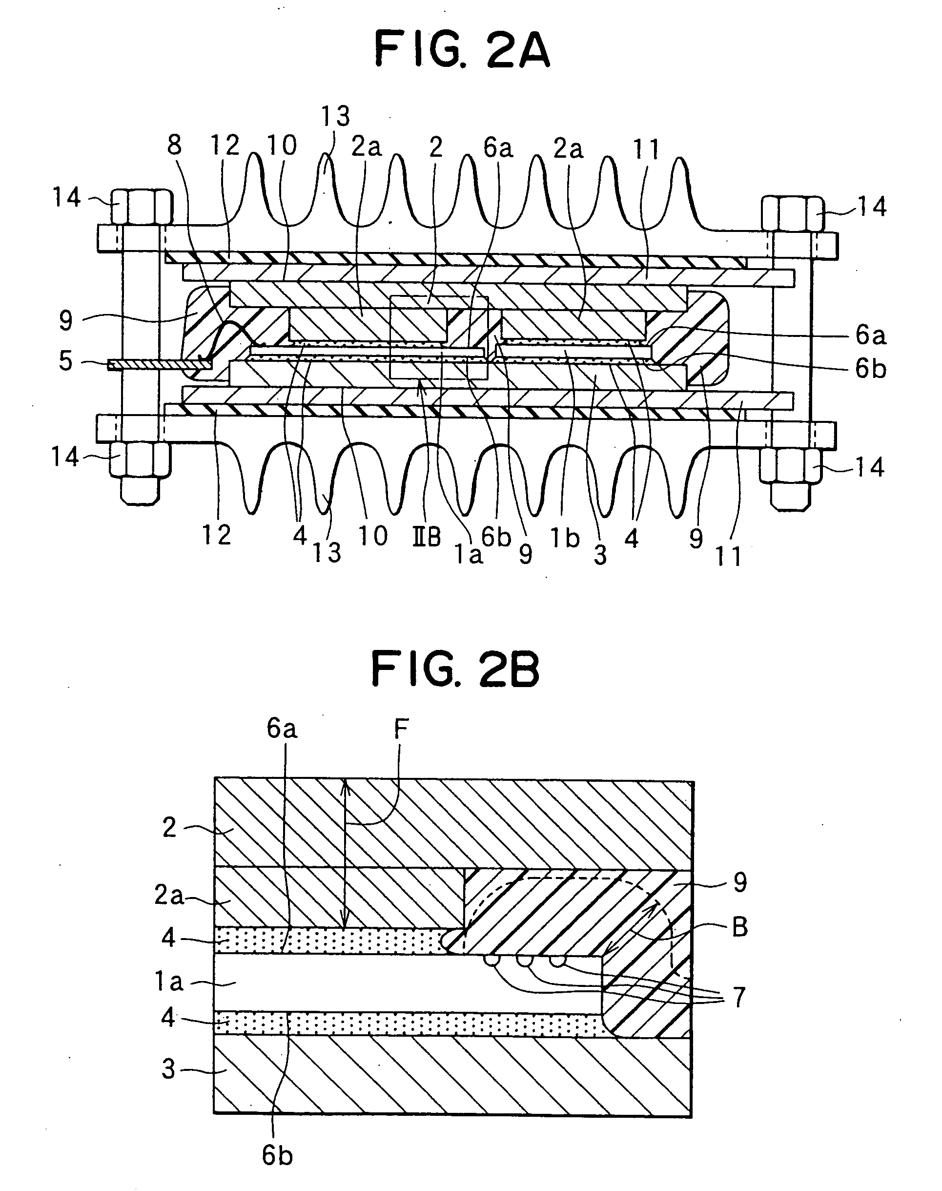
[0062] A first preferred embodiment is described with reference to FIGS. 2A and 2B. As shown in FIG. 2A, a pair of radiation members 2, 3 are disposed to sandwich two Si chips 1a, 1b that are disposed on a plane. The radiation members 2, 3 are thermally and electrically connected to principal electrodes of the Si chips 1a, 1b through bonding members 4. Hereinafter, connection means thermal and electrical connection except cases in which specific descriptions are presented. A control electrode of the Si chip 1a is electrically connected to a control terminal 5, which is connected to a lead frame, via a wire 8 formed by wire bonding.

[0063] Specifically, the radiation member (first side radiation member) 2, facing upper surfaces (first surfaces) 6a of the Si chips 1a, 1b to which the wire bonding is performed is formed with protruding portions 2a protruding at a step-like shape at positions facing the principal electrodes of the Si chips 1a, 1b. Front ends of the protruding portions 2...

second embodiment

[0091] A second preferred embodiment differs from the first embodiment in an inside shape of the first side radiation member 2. FIG. 4A shows a semiconductor device in the second embodiment, and FIGS. 4B to 4D are cross-sectional views partially showing various first side radiation members 2 and Si chips 1a, 1b facing the respective radiation members 2. FIGS. 5A to 5C are cross-sectional views respectively taken along lines VA-VA, VB-VB, VC-VC in FIGS. 4B to 4D.

[0092] In FIG. 4A, the first side radiation member 2 is partially omitted, and the cross-sectional shapes shown in FIGS. 4B to 4D are applicable to the omitted part. FIG. 4A also omits the outside wiring members 11, the high thermal conductivity insulating substrates 12, and the outside cooling members 13. Hereinafter, different portions from those in FIG. 2A are explained. In FIGS. 4A to 4D and 5A to 5C, the same parts as those in FIG. 2A are indicated with the same reference numerals, and those explanation is made simple. ...

third embodiment

[0098]FIG. 6 shows a semiconductor device in a third preferred embodiment, in which the outside wiring members 11, the high thermal conductivity insulating substrates 12, and the outside cooling members 13 shown in FIG. 2A are omitted. Hereinafter, different portions from those in the first embodiment are mainly explained, and in FIG. 6, the same parts as those in FIG. 2A are indicated with the same reference numerals.

[0099] As shown in FIG. 6, in the third embodiment, metallic members (partially disposed metallic members) 16 made of Mo, W, Cu—Mo, or the like having a thermal expansion coefficient approximate to that of Si chips are disposed at the portions of the first side and second side radiation members 2, 3 facing the Si chips 1a, 1b. The partially disposed metallic members 16 can be previously formed on the radiation members 2, 3 by soldering, brazing, shrinkage fitting, or press-fitting. To position the partially disposed metallic members 16 with respect to the Si chips 1a,...


PUM


Abstract

A semiconductor device includes two semiconductor chips that are interposed between a pair of radiation members, and thermally and electrically connected to the radiation members. One of the radiation members has two protruding portions and front ends of the protruding portions are connected to principal electrodes of the semiconductor chips. The radiation members are made of a metallic material containing Cu or Al as a main component. The semiconductor chips and the radiation members are sealed with resin with externally exposed radiation surfaces.

Description

CROSS REFERENCE TO RELATED APPLICATIONS [0001] This application is based upon and claims the benefit of Japanese Patent Applications No. 11-333119 filed on Nov. 24, 1999, No. 11-333124 filed on Nov. 24, 1999, No. 2000-88579 filed on Mar. 24, 2000, No. 2000-97911 filed on Mar. 30, 2000, No. 2000-97912 filed on Mar. 30, 2000 and No. 2000-305228 filed on Oct. 4, 2000, the contents of which are incorporated herein by reference. BACKGROUND OF THE INVENTION [0002] 1. Field of the Invention [0003] This invention relates to a semiconductor device in which heat is radiated from both sides of a semiconductor chip accommodated therein. [0004] 2. Description of the Related Art [0005] For example, JP-A-6-291223 discloses a semiconductor device in which heat is radiated from both sides of a semiconductor chip. FIGS. 1A to 1C show this semiconductor device. As shown in the figures, a pair of radiation members J2, J3 sandwich several semiconductor chips J1, and are thermally and electrically connec...

Claims


Application Information

Patent Timeline
Patent Type & Authority Applications(United States)
IPC IPC(8): H01L23/051H01L23/40H01L23/433
CPCH01L23/051H01L2924/1305H01L23/4334H01L24/32H01L24/33H01L24/73H01L2224/32245H01L2224/48091H01L2224/48247H01L2224/73215H01L2224/73265H01L2924/01003H01L2924/0101H01L2924/01013H01L2924/0102H01L2924/01029H01L2924/0103H01L2924/01042H01L2924/01047H01L2924/0105H01L2924/01052H01L2924/01057H01L2924/01058H01L2924/01061H01L2924/01074H01L2924/01078H01L2924/01079H01L2924/01082H01L2924/01094H01L2924/04941H01L2924/13055H01L2924/30107H01L23/4006H01L2924/1301H01L2924/07811H01L2924/10253H01L2924/1815H01L2924/00013H01L24/48H01L2924/01005H01L2924/01006H01L2924/01019H01L2924/01023H01L2924/01033H01L2924/01068H01L2924/01075H01L2924/01084H01L2924/01322H01L2924/014H01L2924/0132H01L2224/291H01L2924/15747H01L2224/29116H01L2224/29386H01L2224/29111H01L2224/29299H01L2224/2929H01L2224/48472H01L2924/00014H01L2924/3512H01L2924/00H01L2924/0665H01L2924/05442H01L2224/29099H01L2224/29199H01L2924/351H01L2924/181H01L2224/40137H01L24/45H01L2224/05599H01L2224/451H01L2224/85399H01L24/40H01L2224/33H01L2224/37147H01L2224/84801H01L2224/83801H01L24/37H01L2224/40225H01L2224/33181H01L25/072H01L25/18H01L2224/2612H01L24/84H01L2924/00012H01L2224/45015H01L2924/207H01L2224/73221
Inventor MAMITSU, KUNIAKIHIRAI, YASUYOSHI
Owner DENSO CORP
Why Eureka
Try Eureka