Writable tracking cells

a tracking cell and writable technology, applied in the field of nonvolatile semiconductor memory devices, can solve the problems of system write speed most often limited by user cells, and achieve the effect of reducing the uncertainty of the final written threshold of the reference cell and less uncertainty in the final written threshold of the tracking cell

Active Publication Date: 2005-08-04
SANDISK TECH LLC
View PDF5 Cites 103 Cited by
  • Summary
  • Abstract
  • Description
  • Claims
  • Application Information

AI Technical Summary

Benefits of technology

[0011] A set of alternate embodiments provide for using different voltages and / or timing for the writing of tracking cells to provide less uncertainty in the tracking cells' final written thresholds. Since there are typically many fewer tracking cells than user storage cells, system write speed is most often limited by the user cells, not the reference cells. Therefore, it may be possible to use different voltages and / or timings which write the reference cells more slowly on average while still writing the slowest reference cell as quickly as the slowest user cell. This can reduce reference cell threshold uncertainty without significantly effecting the overall system write speed.

Problems solved by technology

Since there are typically many fewer tracking cells than user storage cells, system write speed is most often limited by the user cells, not the reference cells.

Method used


Image

  • Writable tracking cells
  • Writable tracking cells
  • Writable tracking cells

Examples


Embodiment Construction

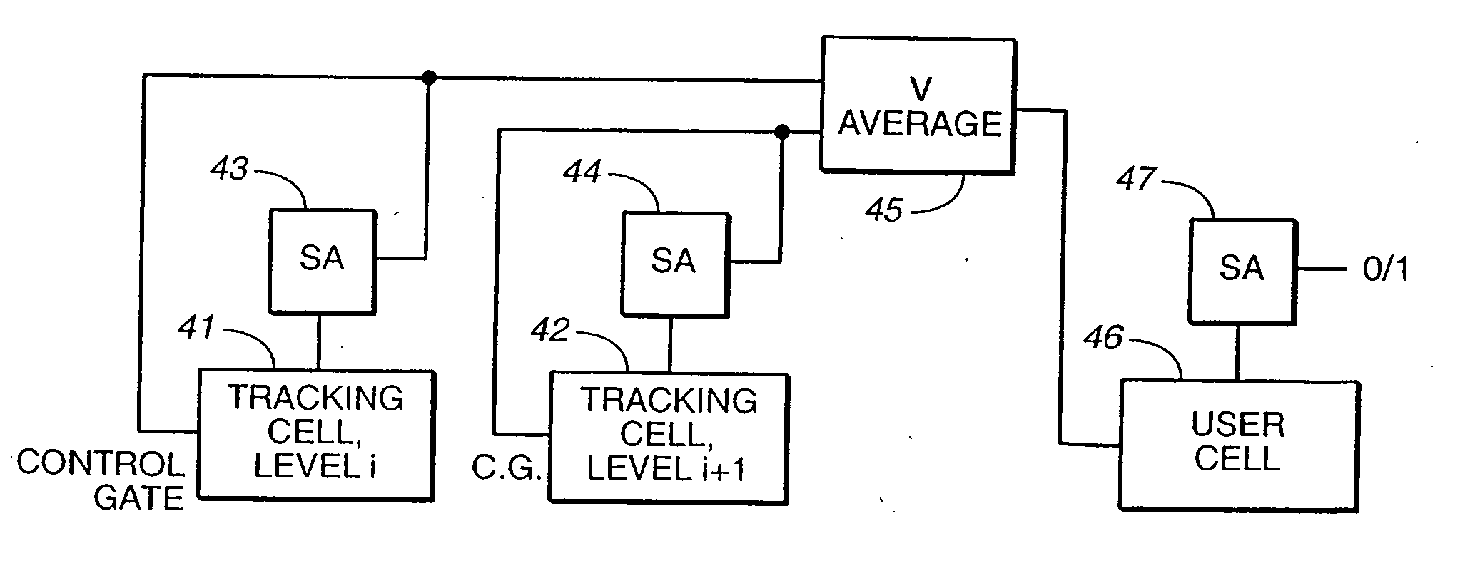
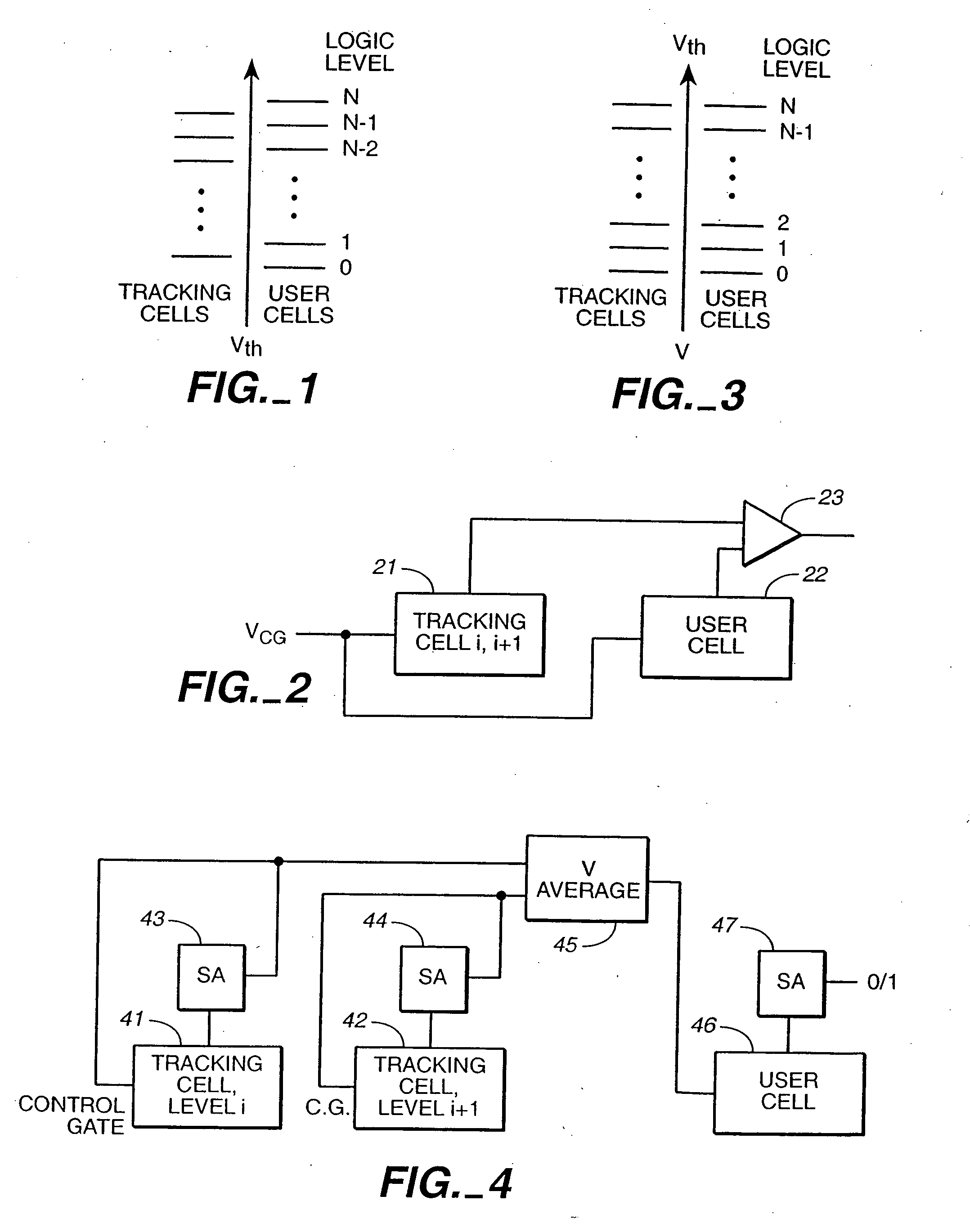
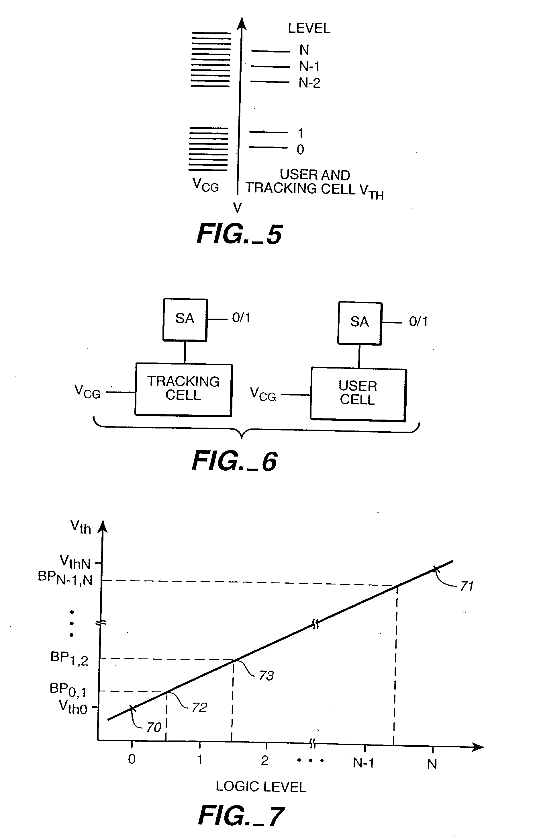
[0028] The storage capacity of non-volatile semiconductor memories has increased both by the reduction in size of the individual components of the circuits and by increasing the amount of data storable in an individual memory cell. For example, devices such as those described in U.S. Pat. Nos. 5,712,189 and 6,103,573 and U.S. patent application Ser. No. 09 / 505,555, filed on Feb. 17, 2000, and one entitled “Non-Volatile Memory Cell Array Having Discontinuous Drain and Source Diffusions Contacted by Continuous Bit Line Conductors and Methods of Forming” by Jack H. Yuan and Jacob Haskell, field on Sep. 22, 2000, which are all assigned to SanDisk Corporation and which are all hereby incorporated herein by this reference, can store upwards of four logical bits per physical floating gate storage transistor. This storage will require each floating gate to be able to have encoded within it one of the sixteen or more possible memory states. Each one of these memory states corresponds to a un...


PUM


Abstract

The present invention presents several techniques for using writable tracking cells. Multiple tracking cells are provided for each write block of the memory. These cells are re-programmed each time the user cells of the associated write block are written, preferably at the same time, using the same fixed, global reference levels to set the tracking and user cell programmed thresholds. The threshold voltages of the tracking cells are read every time the user cells are read, and these thresholds are used to determine the stored logic levels of the user cells. In one set of embodiments, populations of one or more tracking cells are associated with different logic levels of a multi-state memory. These tracking cell populations may be provided for only a subset of the logic levels. The read points for translating the threshold voltages are derived for all of the logic levels based upon this subset. In one embodiment, two populations each consisting of multiple tracking cells are associated with two logic levels of the multi-bit cell. In an analog implementation, the user cells are read directly using the analog threshold values of the tracking cell populations without their first being translated to digital values. A set of alternate embodiments provide for using different voltages and/or timing for the writing of tracking cells to provide less uncertainty in the tracking cells' final written thresholds.

Description

BACKGROUND OF THE INVENTION [0001] 1. Field of the Invention [0002] The present invention relates generally to non-volatile semiconductor memory devices and, more particularly, to the use of tracking cells for the reading of multi-state memories. [0003] 2. Background Information [0004] In a semiconductor memory cell, data is stored by programming the cell to have a desired threshold voltage. The data stored in the cell is read by determining the threshold voltage of the cell and translating this voltage to a logic level. For a two state, binary memory cell, this translation can be done by use of a reference or breakpoint voltage to provide a read point: cells with a threshold voltage above this read point correspond to one state, while those with a threshold voltage below this read point correspond to the other state. When a memory cell is a multi-state cell, a number of such read points need to be introduced to distinguish between the states. [0005] As the number of states stored i...

Claims


Application Information

Patent Timeline
Patent Type & Authority Applications(United States)
IPC IPC(8): G11C7/06G11C7/14G11C11/34G11C11/56G11C27/00
CPCG11C7/06G11C7/14G11C2211/5634G11C27/005G11C11/5642
Inventor KHALID, SHAHZAD B.GUTERMAN, DANIEL C.GONGWER, GEOFFREY S.SIMKO, RICHARDCONLEY, KEVIN M.
Owner SANDISK TECH LLC
Why Eureka
Try Eureka