Automatic placement and routing device, method for placement and routing of semiconductor device, semiconductor device and manufacturing method of the same

a technology of automatic placement and routing, which is applied in the direction of computer aided design, program control, instruments, etc., can solve the problems of affecting routing efficiency, spare cells giving load, and huge spare cells, so as to reduce the load of routing tools and the memory capacity required

Inactive Publication Date: 2005-08-04
NEC ELECTRONICS CORP
View PDF15 Cites 13 Cited by
  • Summary
  • Abstract
  • Description
  • Claims
  • Application Information

AI Technical Summary

Benefits of technology

[0008] Therefore, an object of the present invention is to provide an automatic placement and routing device and a method of placement and routing of a semiconductor device, which can places spare cells while reducing the load

Problems solved by technology

However, since the number of the spare cells is huge, the spare cells give a load to the routing tool of the aut

Method used


Image

  • Automatic placement and routing device, method for placement and routing of semiconductor device, semiconductor device and manufacturing method of the same
  • Automatic placement and routing device, method for placement and routing of semiconductor device, semiconductor device and manufacturing method of the same
  • Automatic placement and routing device, method for placement and routing of semiconductor device, semiconductor device and manufacturing method of the same

Examples


Embodiment Construction

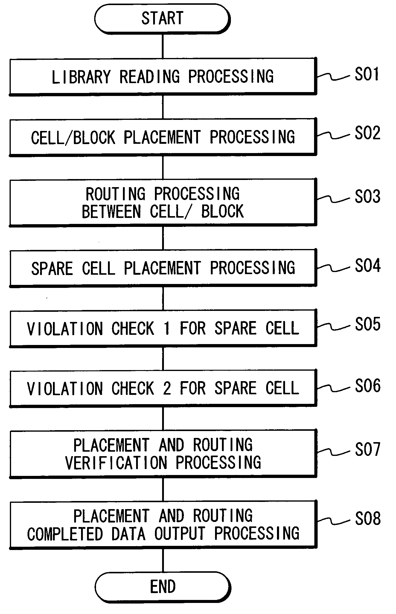
[0039] Embodiments of an automatic placement and routing device, a method of the placement and routing in the semiconductor device, a manufacturing method of the semiconductor device of the present invention will be described below with reference to the attached drawings. It should be noted that both of a (logic) functional cell and a (logic) functional block are referred to as a functional block in following specification.

[0040] Firstly, a configuration of the embodiment of the automatic placement and routing device of the present invention, to which the method of the placement and routing of the semiconductor device is applied, will be described with reference to the attached drawings.

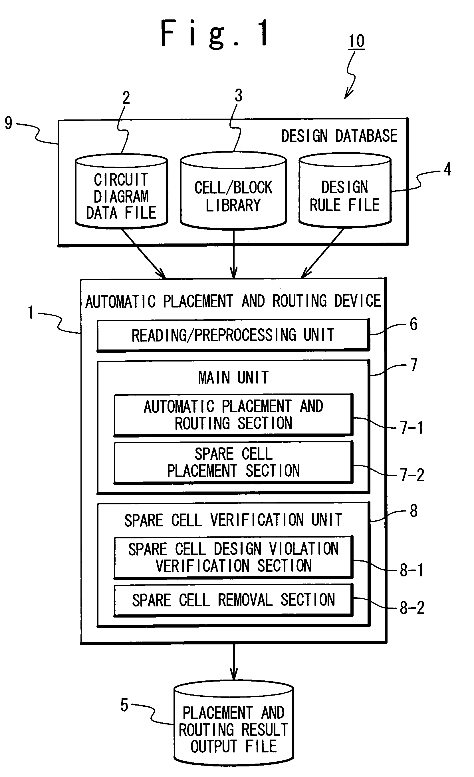
[0041]FIG. 1 is a view showing the configuration of the embodiment of the automatic placement and routing device according to the present invention. A placement and routing system 10 includes an automatic placement and routing device 1 and a design database 9.

[0042] The design database 9 is an inf...


PUM


Abstract

A method of placement and routing of a semiconductor device, includes steps (a) to (c). The step (a) is a procedure of executing placement of functional blocks and executing routing of interconnections in a placement and routing area of a semiconductor device based on circuit diagram data, functional block data and design rule data. The step (b) is a procedure of executing placement of spare cells in first areas of the placement and routing area, disregarding the routing result, wherein the functional blocks are not placed in the first areas, the spare cells are spare functional blocks. The step (c) is a procedure of removing first spare cells of the spare cells from the first areas, wherein the first spare cells are in violation of a design rule with regard to a relation to the interconnections, the design rule is described in the design rule data.

Description

BACKGROUND OF THE INVENTION [0001] 1. Field of the Invention [0002] The present invention relate to an automatic placement and routing device, a method of placement and routing of a semiconductor device, a semiconductor device and a manufacturing method of the same. More particularly, the present invention relates to those devices and methods which are improved in an efficiency of the designing semiconductor devices. [0003] 2. Description of the Related Art [0004] In a layout design of a large-scale integration (LSI), an automatic placement and routing system is known, in which placing functional blocks and the routing are carried out automatically. In the following description, both of a (logic) functional cell and a (logic) functional block are referred to as a functional block. A computer having a CAD (Computer Aided Design) software exemplifies the automatic placement and routing device. A placement and routing using the automatic placement and routing device is carried out, for...

Claims


Application Information

Patent Timeline
IPC IPC(8): G06F17/50H01L21/82H01L27/00
CPCG06F17/5077G06F17/5072G06F30/394G06F30/392
Inventor OSANAI, AYUMU
Owner NEC ELECTRONICS CORP
Why Eureka
Try Eureka