
Full-color organic display having improved blue emission

a full-color organic display and blue emission technology, applied in the field of improving the performance can solve the problems of limited life of full-color organic displays, achieve the effects of increasing the luminous efficiency of the display, reducing the surface emitting area, and increasing the lifetim

Active Publication Date: 2005-08-11
GLOBAL OLED TECH
View PDF18 Cites 127 Cited by
  • Summary
  • Abstract
  • Description
  • Claims
  • Application Information

AI Technical Summary

Benefits of technology

[0006] It is therefore an object of the present invention to improve the lifetime of a blue light-emitting subpixel in each pixel of a full-color organic display.
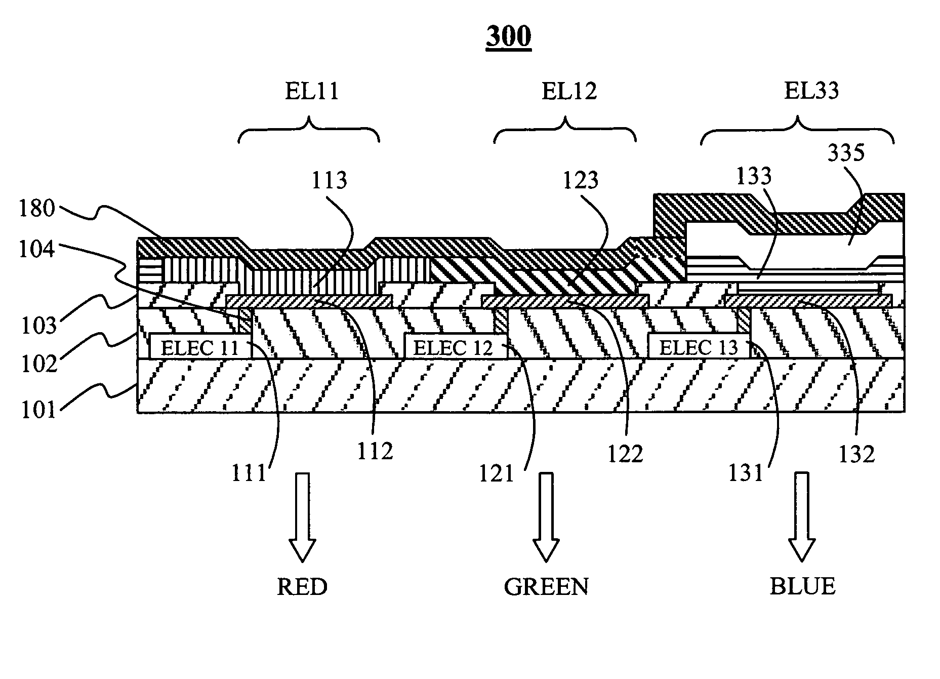
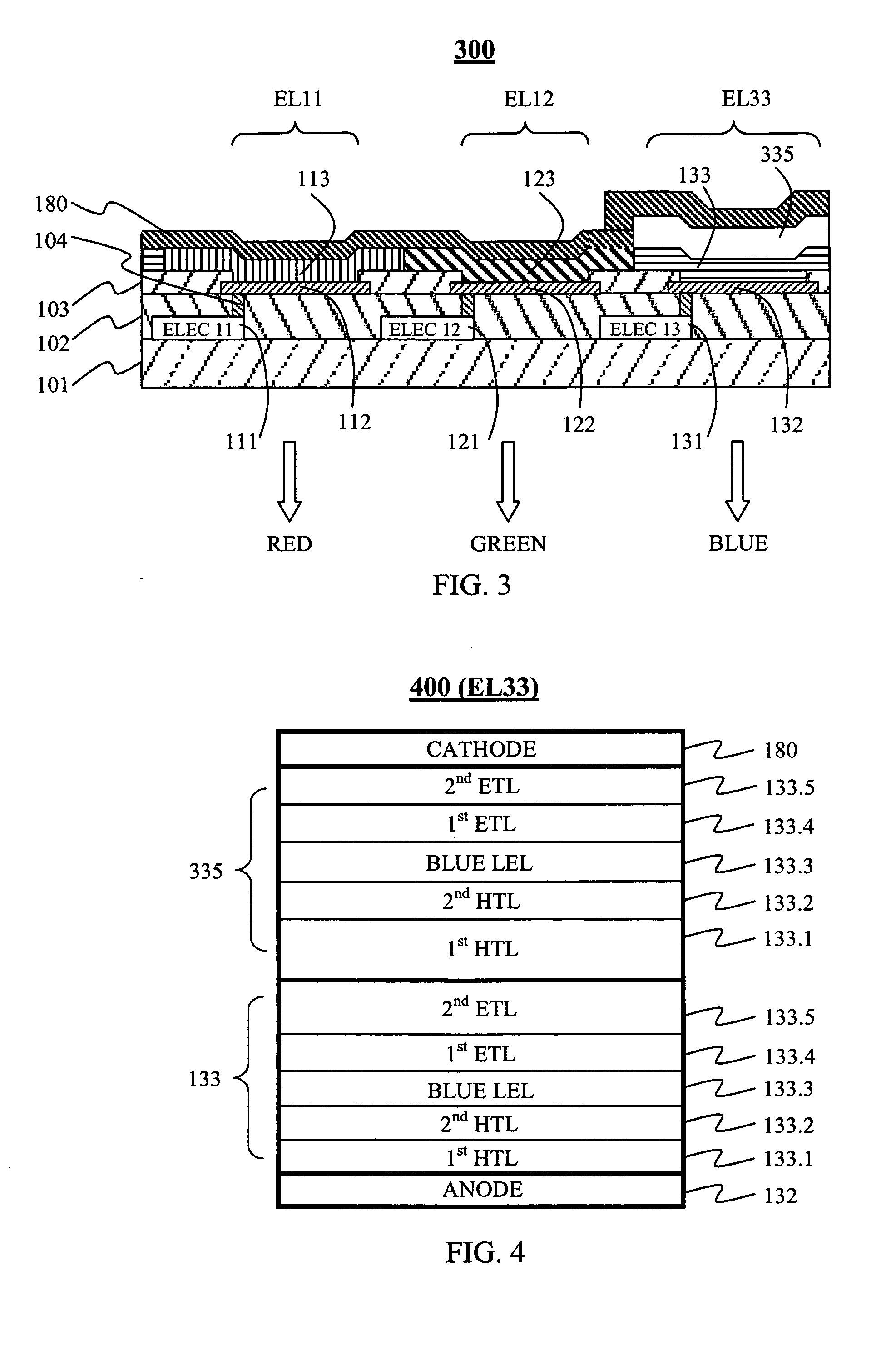
[0008] The present invention makes use of a plurality of vertically stacked EL units in a blue light-emitting subpixel. A blue light-emitting subpixel having a plurality of EL units can increase its luminous efficiency by a factor of the number of the EL units. As a result, its lifetime can be increased with the increase in the number of the EL units at a same brightness, without necessarily increasing its own surface emitting area and decreasing the surface emitting areas of the other EL subpixels in a pixel.

Problems solved by technology

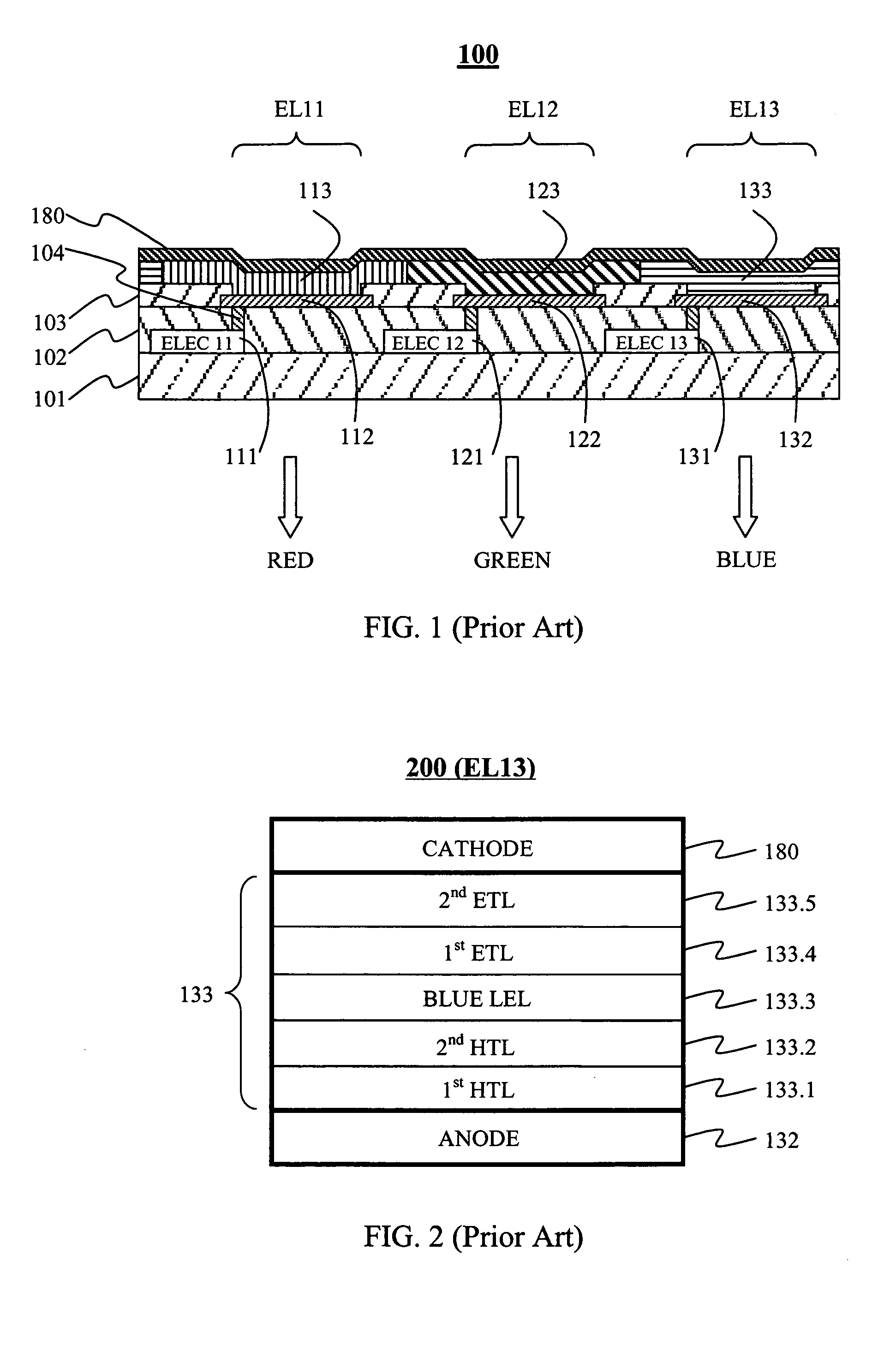
Obviously, the lifetime of a full-color organic display is limited by the blue EL subpixel.

Method used


Image

  • Full-color organic display having improved blue emission
  • Full-color organic display having improved blue emission
  • Full-color organic display having improved blue emission

Examples


example 1

Comparative

[0124] The preparation of a conventional blue EL subpixel is as follows: A ˜1.1 mm thick glass substrate coated with a transparent ITO conductive layer was cleaned and dried using a commercial glass scrubber tool. The thickness of ITO is about 42 nm and the sheet resistance of the ITO is about 68 Ω / square. The ITO surface was subsequently treated with oxidative plasma to condition the surface as an anode. A layer of CFx, 1 nm thick, was deposited on the clean ITO surface as the HIL by decomposing CHF3 gas in an RF plasma treatment chamber. The substrate was then transferred into a vacuum deposition chamber (TROVATO MFG. INC) for deposition of all other layers on top of the substrate. The following layers were deposited in the following sequence by evaporation from a heated boat under a vacuum of approximately 10−6 Torr: [0125] 1. EL unit: [0126] (1) a first HTL, about 70 nm thick, consisting of m-TDATA doped with 3.0 vol. % F4-TCNQ; [0127] (2) a second HTL, 10 nm thick, ...

example 2

[0133] A blue EL subpixel was constructed in the manner described in Example 1, and the deposited layer structure is: [0134] 1. 1st EL unit: [0135] (1) a first HTL, about 70 nm thick, consisting of m-TDATA doped with 3.0 vol. % F4-TCNQ; [0136] (2) a second HTL, 10 nm thick, consisting of NPB; [0137] (3) a LEL, 20 nm thick, consisting of TBADN doped with 1.5 vol. % TBP; [0138] (4) a first ETL, 10 nm thick, consisting of Bphen; and [0139] (5) a second ETL, 25 nm thick, consisting of Bphen doped with 1.2 vol. % Li. [0140] 2. 2nd EL unit: [0141] (1) a first HTL, about 55 nm thick, consisting of m-TDATA doped with 3.0 vol. % F4-TCNQ; [0142] (2) a second HTL, 10 nm thick, consisting of NPB; [0143] (3) a LEL, 20 nm thick, consisting of TBADN doped with 1.5 vol. % TBP; [0144] (4) a first ETL, 10 nm thick, consisting of Bphen; and [0145] (5) a second ETL, 25 nm thick, consisting of Bphen doped with 1.2 vol. % Li. [0146] 3. Cathode: approximately 330 nm thick, consisting of MgAg.

[0147] The E...


PUM


Abstract

A full-color organic display for displaying a color image, including an array of pixels arranged in repeating patterns, wherein each pixel has red, green, and blue light-emitting subpixels, and wherein each red and green light-emitting subpixel contains only one EL unit, while each blue light-emitting subpixel contains more than one vertically stacked EL unit.

Description

FIELD OF INVENTION [0001] The present invention relates to improving the performance of a full-color organic display, and more particularly to improving the lifetime of the blue light-emitting subpixel in each of the pixels in a full-color organic display. BACKGROUND OF THE INVENTION [0002] There is an array of pixels in a full-color organic display (also known as an organic light-emitting display). Each pixel can include red, green, and blue electroluminescence (EL) subpixels (commonly referred to as light-emitting subpixels, RGB subpixels, or RGB elements). Each light-emitting subpixel consists of a basic organic light-emitting diode (OLED). The basic OLED has in common an anode, a cathode, and an organic EL medium (or EL unit) sandwiched between the anode and the cathode. The organic EL medium can include one or more layers of organic thin films, where one of the layers is primarily responsible for EL or light emission. This particular layer is generally referred to as the light-...

Claims


Application Information

Patent Timeline
IPC IPC(8): H01L27/32H01L51/50H01L51/52
CPCH01L27/3211H01L51/5278H01L51/5052H10K59/35H10K50/155H10K50/165H10K50/19
Inventor LIAO, LIANG-SHENGKLUBEK, KEVIN P.TANG, CHING W.
Owner GLOBAL OLED TECH
Learn More