
Use of gate electrode workfunction to improve DRAM refresh

a gate electrode and workfunction technology, applied in semiconductor devices, digital storage, instruments, etc., can solve the problems of increasing the doping level of the underlying channel region of the substrate, increasing current leakage, and aggravated efforts to alleviate one leakage problem, so as to reduce the doping requirements of the array substrate channel region, reduce and minimize the effect of transistor and diode current leakag

Inactive Publication Date: 2005-08-11
MICRON TECH INC
View PDF16 Cites 4 Cited by
  • Summary
  • Abstract
  • Description
  • Claims
  • Application Information

AI Technical Summary

Benefits of technology

This approach enables the formation of DRAM transistors with tailored threshold voltages and reduced leakage, enhancing refresh performance by minimizing transistor and diode current leakage while maintaining sufficient switching performance.

Problems solved by technology

In semiconductor device manufacture, a known problem is that as gate lengths of transistors are scaled to shorter and shorter lengths and gate dielectrics are reduced, the doping levels of the underlying channel region of the substrate must be increased to maintain sufficient access device threshold voltages (Vt).
Current leakage is a problem with modern memory devices associated with such doping.
A major problem is that efforts to alleviate one leakage problem worsens the other.
Hence, when access devices are manufactured by current processes, they must be designed to balance theses two leakage components, which is becoming increasingly more difficult to do.
Another problem is that as the array (channel region) doping levels increase in a DRAM array to set sufficient threshold voltage for the access transistor, DRAM refresh characteristics suffer.

Method used


Image

  • Use of gate electrode workfunction to improve DRAM refresh
  • Use of gate electrode workfunction to improve DRAM refresh
  • Use of gate electrode workfunction to improve DRAM refresh

Examples


embodiment 1

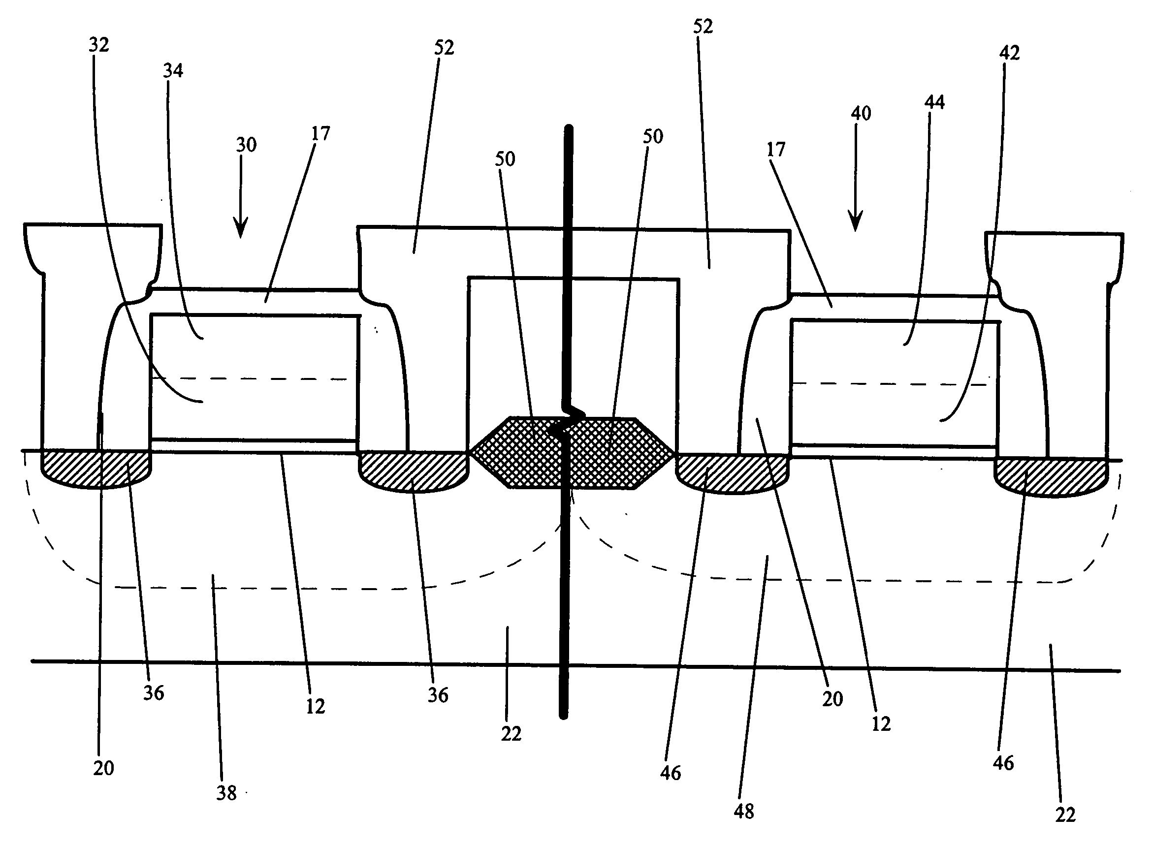
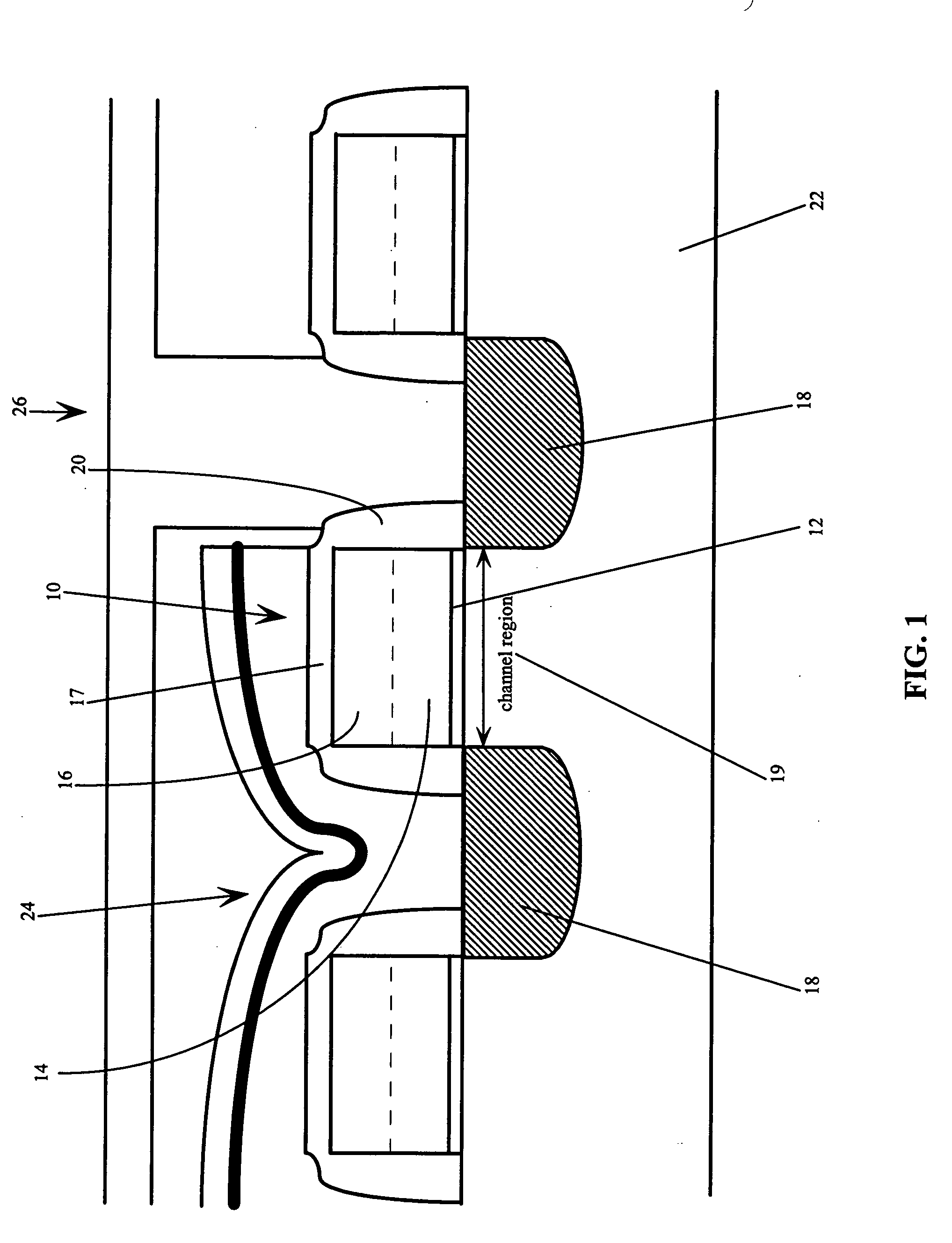
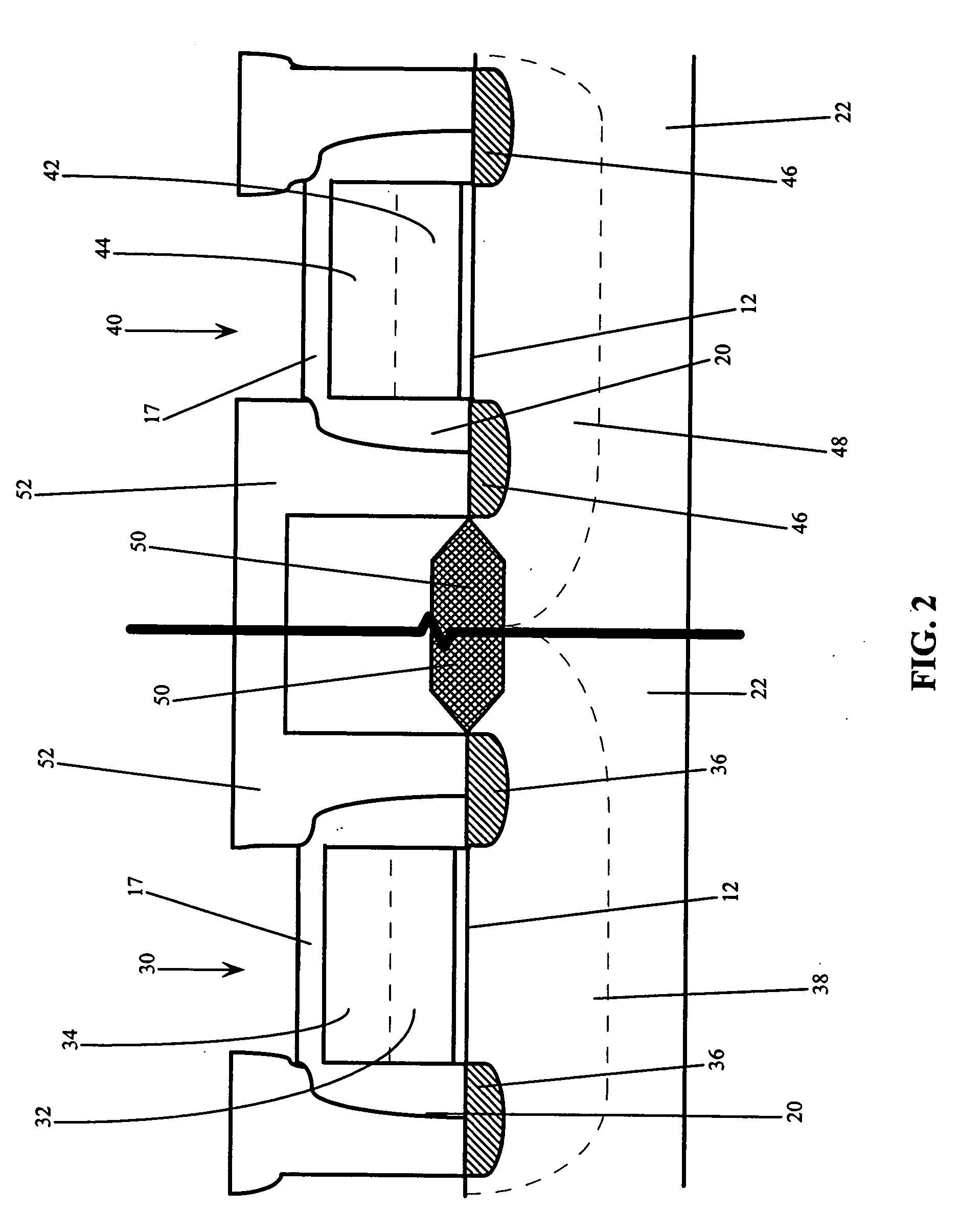
[0036] In the first embodiment, the semiconductor device structure has access transistors comprising P+ Si / Ge gate electrodes 14, periphery NMOS transistors comprising P+ Si / Ge gate electrodes 32 and periphery PMOS transistors comprising P+ Si / Ge gate electrodes 42.

embodiment 2

[0037] In the second embodiment, the semiconductor device structure has access transistors comprising P+ Si / Ge gate electrode 14, a majority of periphery NMOS transistors comprise N+ Si / Ge gate electrodes 32, and a minority of periphery NMOS transistors comprise P+ Si / Ge gate electrodes 32, and a majority of the periphery PMOS transistors comprise P+ Si / Ge gate electrode 42, and a minority comprise N+ Si / Ge gate electrodes 42.

embodiment 3

[0038] For the third embodiment, the semiconductor device structure has access transistors comprising either N+ or P+ Si / Ge gate electrodes 14, a majority of periphery NMOS transistors comprise a N+ poly gate electrodes 32, and may have a minority comprise either P+ poly or Si / Ge gate electrodes 32, and periphery PMOS transistors comprise either P+ poly or N+ poly gate electrodes 42.


PUM


Abstract

This invention relates to a method and resulting structure, wherein a DRAM may be fabricated by using silicon midgap materials for transistor gate electrodes, thereby improving refresh characteristics of access transistors. The threshold voltage may be set with reduced substrate doping requirements. Current leakage is improved by this process as well.

Description

FIELD OF THE INVENTION [0001] This invention relates to the field of semiconductor memory circuits, and particularly to a method of improving DRAM refresh by using midgap or near midgap materials, such as silicon germanium, in transistor gate electrodes for tuning workfunction and threshold voltages in DRAM access transistors, so as to minimize current leakage. BACKGROUND OF THE INVENTION [0002] Doping of semiconductor substrates to form semiconductor devices is a well known practice in the art. To form memory devices, not only are the underlying substrate and source and drain regions implanted with dopant, but most often the conductive elements of the transistor gates are doped as well. In modern DRAM processing, typical and almost universal doping patterns for transistors in the prior art include utilizing a N+ doped polysilicon (poly) for the access transistor gates, N+ doped poly for periphery NMOS transistor gates, and N+ doped poly for periphery PMOS transistor gates. A new tr...

Claims


Application Information

Patent Timeline
Patent Type & Authority Applications(United States)
IPC IPC(8): G11C11/406H10B12/00
CPCG11C11/406H01L27/10873H01L27/10811H10B12/312H10B12/05
Inventor DENNISON, CHARLES H.
Owner MICRON TECH INC
Learn More