Apparatus and method for controlling enable time of signal controlling operation of data buses of memory device

Active Publication Date: 2005-08-11
SK HYNIX INC
View PDF8 Cites 7 Cited by
  • Summary
  • Abstract
  • Description
  • Claims
  • Application Information

AI Technical Summary

Benefits of technology

[0021] Still another object of the present invention is to provide a method for delaying a pulse signal outputted from the read / write strobe pulse generating circuit and for controlling the width of the pulse signal by applying an external address signal during a test mode.

Problems solved by technology

However, such a conventional method may cause an expensive cost and much time.

Method used


Image

  • Apparatus and method for controlling enable time of signal controlling operation of data buses of memory device
  • Apparatus and method for controlling enable time of signal controlling operation of data buses of memory device
  • Apparatus and method for controlling enable time of signal controlling operation of data buses of memory device

Examples


Embodiment Construction

[0036] Hereinafter, a preferred embodiment of the present invention will be described with reference to the accompanying drawings. In the following description and drawings, the same reference numerals are used to designate the same or similar components, and so repetition of the description on the same or similar components will be omitted.

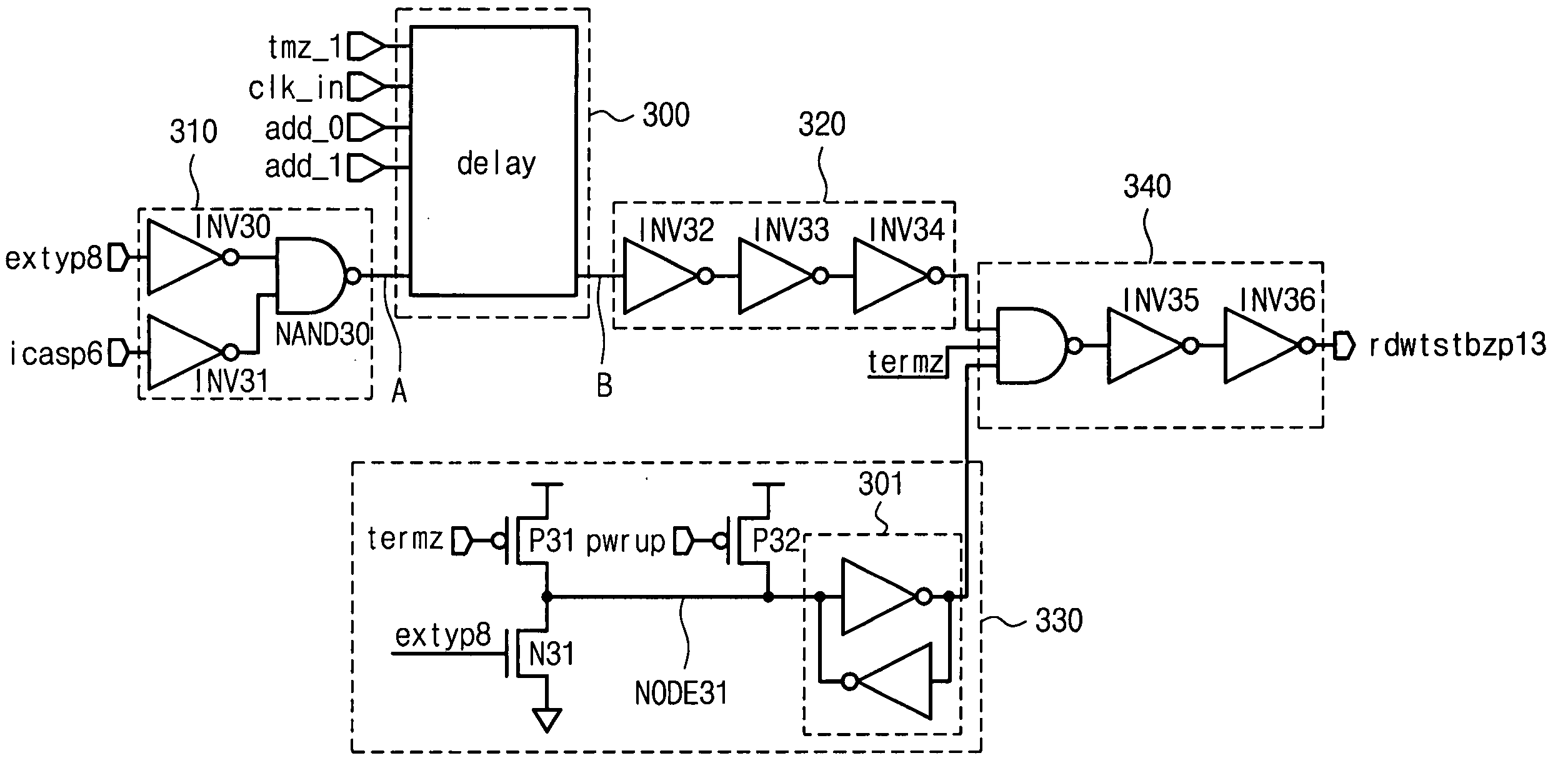
[0037]FIG. 3 is a circuit diagram illustrating a read / write strobe pulse generating circuit according to one embodiment of the present invention.

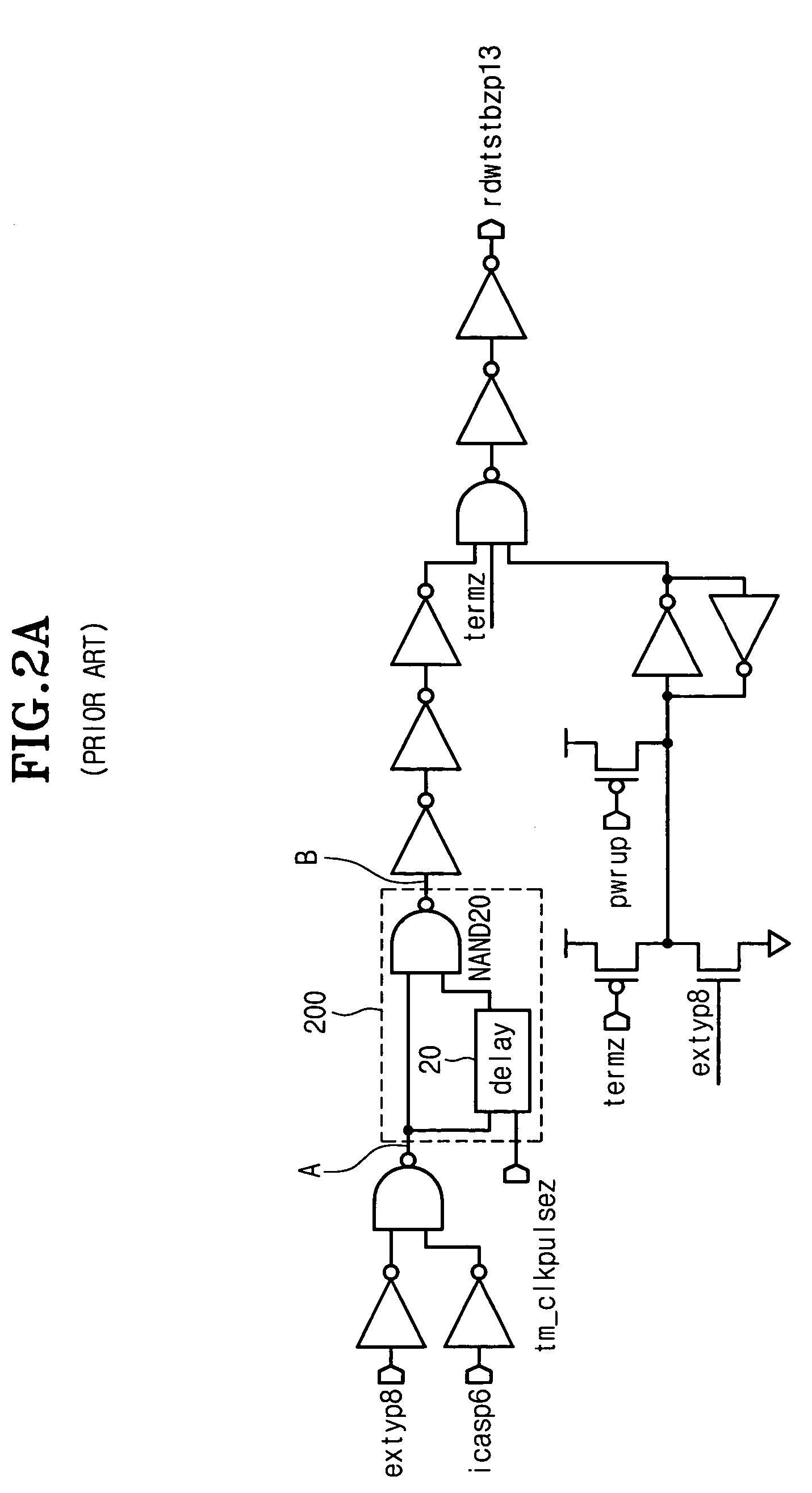
[0038] In comparison with the circuit of FIG. 2A, the circuit shown in FIG. 3 has a different feature in that a pulse width control section 300 is controlled by a clock signal “clk-in”.

[0039] The circuit of FIG. 3 includes an input signal receiving section 310, the pulse width control section 300, a signal transmission section 320, a circuit section 330 for a test mode, and an output section 340.

[0040] The input signal receiving section 310 includes inverters INV30 and INV31 and a NAND gate NAND30. A...


PUM


Abstract

Disclosed is an apparatus for controlling an enable interval of a signal controlling an operation of data buses which connect a bit line sense amplifier with a data sense amplifier according to a variation of an operational frequency of a memory device. The apparatus comprises a pulse width control section for changing the pulse width of an input signal depending on the operational frequency of the memory device after receiving the input signal, a signal transmission section for buffering a signal outputted from the pulse width control section, and an output section for receiving a signal outputted from the signal transmission section so as to output a first signal for controlling the signal to control the operation of the data buses.

Description

BACKGROUND OF THE INVENTION [0001] 1. Field of the Invention [0002] The present invention relates to a method for controlling the operation of a sense amplifier for a memory device, and more particularly to a method capable of controlling an operation period of a sense amplifier according to variation of an operational frequency of a memory device. [0003] 2. Description of the Prior Art [0004]FIG. 1 is a view for explaining a read operation and a write operation of a general memory device. [0005] As shown in FIG. 1, during the write operation, data applied through an input / output data pad are transferred to a bit line sense amplifier through a data input buffer, a data input register, and a write driver. Also, during the read operation, cell data amplified by the bit line sense amplifier are transferred to the input / output data pad through a data sense amplifier, a pipe register, and a data output buffer. [0006] In FIG. 1, signal “Yi” is a pulse signal for controlling the operation ...

Claims


Application Information

Patent Timeline
IPC IPC(8): G11C7/00G11C7/08G11C7/10
CPCG11C7/1072G11C7/222G11C2207/2254G11C29/50012G11C29/028G11C7/08
Inventor KIM, JI HYUNNAM, YOUNG JUN
Owner SK HYNIX INC
Why Eureka
Try Eureka