

Light emitting element, method for manufacturing light emitting element, light emitting element assembly, and method for manufacturing light emitting element assembly
- Summary
- Abstract
- Description
- Claims
- Application Information
AI Technical Summary
Benefits of technology
Problems solved by technology
Method used
Image

Examples
example 1
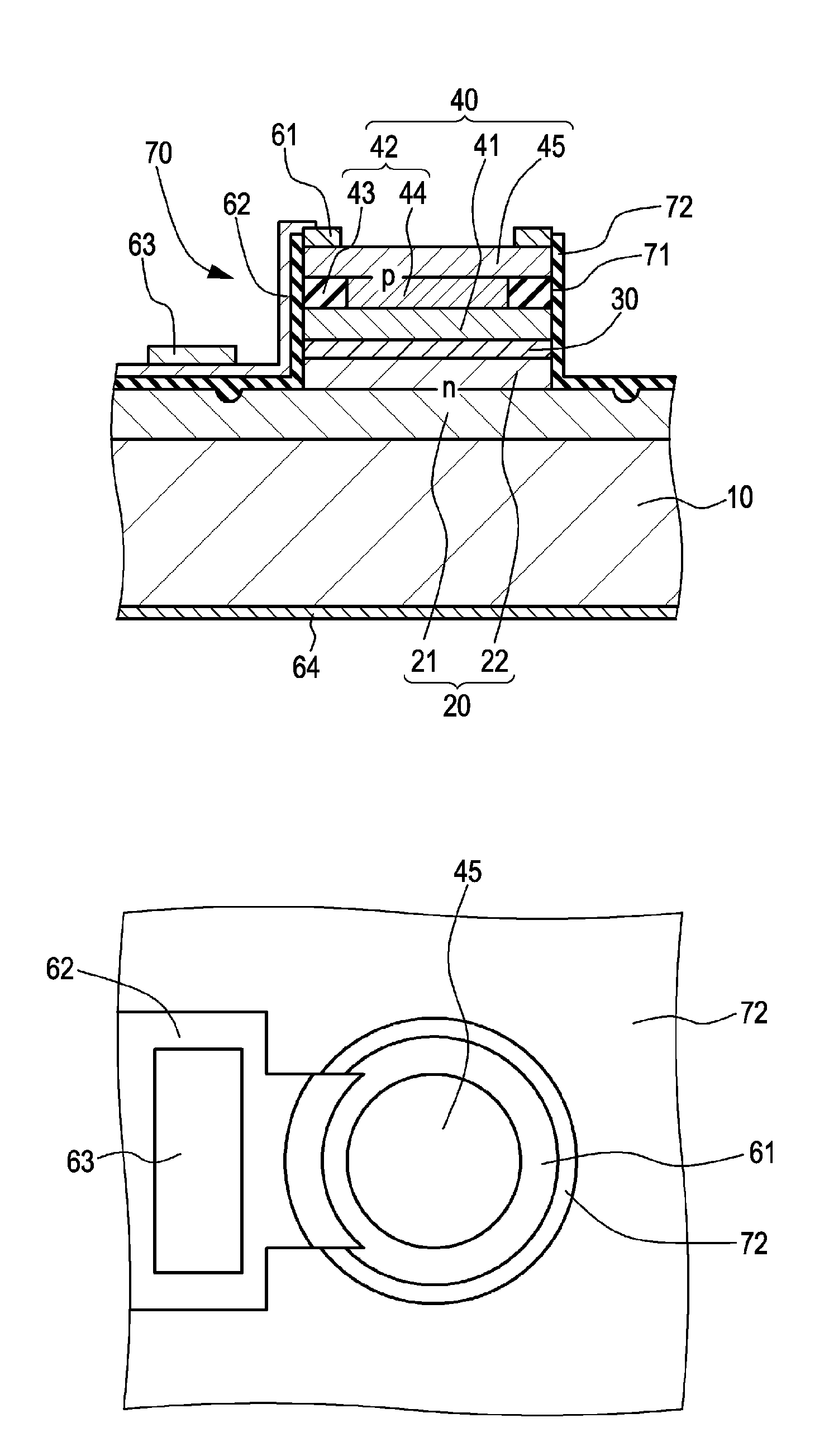
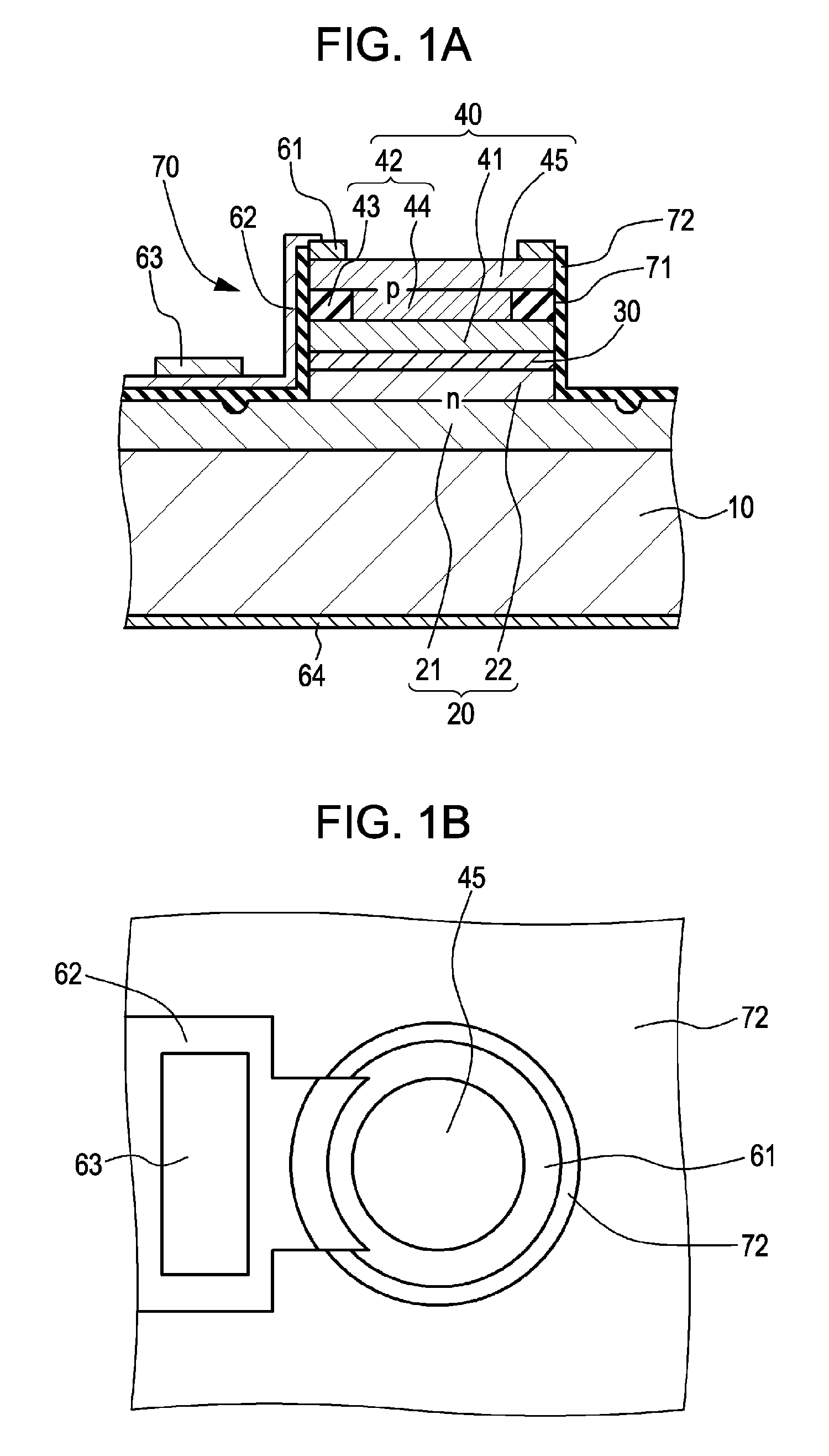
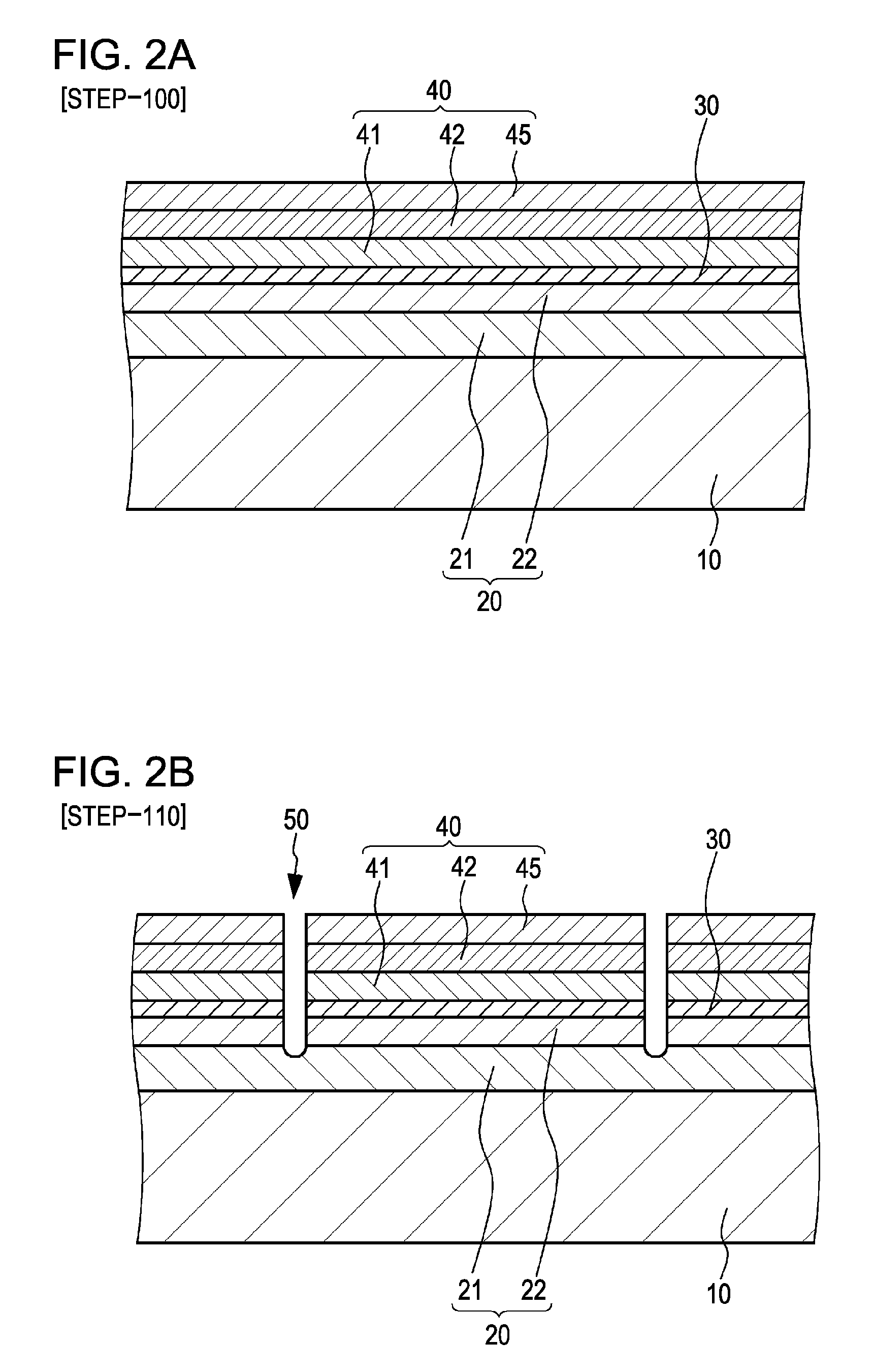
[0048]Example 1 relates to a light emitting element and a method for manufacturing the light emitting element according to embodiments of the present invention. FIG. 1A is a schematic partial sectional view of the light emitting element in Example 1 and FIG. 1B is a schematic partial plan view. In Example 1 or in Example 2 or Example 3 described later, a first conduction type is specified to be an n-type and a second conduction type is specified to be a p-type. In Example 1 or in Example 2 or Example 3 described later, the light emitting element is composed of a surface emitting laser element (vertical cavity surface emitting laser, VCSEL) for emitting light through a second compound semiconductor layer.
[0049]The light emitting element in Example 1 or in Example 2 or Example 3 described later is composed of a first compound semiconductor layer 20, an active layer 30, and a second compound semiconductor layer 40 disposed on a substrate 10 formed from an n-type GaAs substrate. The fir...
example 2
[0068]Example 2 relates to a light emitting element assembly and a method for manufacturing the light emitting element assembly according to embodiments of the present invention. FIG. 9 is a schematic partial plan view of the light emitting element assembly in Example 2. Each light emitting element in Example 2 has the same configuration and structure as those of the light emitting element described in Example 1. Therefore, detailed explanations will not be provided.
[0069]In Example 2, K1 light emitting elements (K1 mesa structures 70) are disposed in each region 80 to be provided with a light emitting element assembly. Specifically, K0 is specified to be four, and K1 is specified to be one in Example 2. Circles with reference numeral 70A are indicated by a dotted line and show (K0−K1) units of current confinement regions which have not been used for constituting the light emitting element. The areas of K0 current confinement regions are differentiated from each other, although the ...
example 3
[0084]Example 3 is a modification to Example 2. In Example 2, K0 is specified to be four, and K1 is specified to be one. On the other hand, K0 is specified to be thirty-two, and K1 is specified to be eight in example 3. In each region 80 to be provided with a light emitting element assembly, thirty-two current confinement regions 44 are formed and, thereafter, eight mesa structures 70 are left. The areas of current confinement regions 44 in eight mesa structures 70 are nearly equal. In general, a laser array is composed of laser elements having the same characteristics. That is, it is ideal that the areas of current confinement regions 44 in finally formed eight mesa structures 70 are equal. If the values of diameter R0 of the regions to be provided with the mesa structure are equal, the areas of the formed current confinement regions 44 are supposed to become nearly equal. However, it may be difficult to allow the area of the current confinement region 44 to become an intended valu...
PUM
 Abstract
Description
Claims
Application Information