Single Crystal Semiconductor Manufacturing Apparatus and Manufacturing Method

Active Publication Date: 2009-05-28
SUMCO TECHXIV
View PDF6 Cites 4 Cited by
  • Summary
  • Abstract
  • Description
  • Claims
  • Application Information

AI Technical Summary

Benefits of technology

[0021]According to the above method 1), the control width of the oxygen concentration in the single crystal silicon is narrow, and the yield of the single crystal silicon is low.
[0022]According to the above method 2), the cost for introduction of the magnetic field generation device and the cost for its maintenance and management are very high, so that it is hard to manufacture semiconductor products at a low cost.
[0023]Meanwhile, the method of controlling the oxygen concentration in the single crystal silicon by the plural heaters can make the control width of the oxygen concentration in the single crystal silicon somewhat larger than the above method 1) and can improve the yield of the single crystal silicon though only slightly. And, the cost does not become as high as that for the above method 2).

Problems solved by technology

Therefore, mere adjustment of the electric power supplied to the single heater 10 is virtually hard to provide a uniform oxygen concentration in the growing direction of the single crystal silicon 6 because the control width of the oxygen concentration in the single crystal silicon 6 is very small.

Method used


Image

  • Single Crystal Semiconductor Manufacturing Apparatus and Manufacturing Method
  • Single Crystal Semiconductor Manufacturing Apparatus and Manufacturing Method
  • Single Crystal Semiconductor Manufacturing Apparatus and Manufacturing Method

Examples


Embodiment Construction

[0084]Embodiments of a single crystal semiconductor manufacturing apparatus of the present invention and a heater used therefor will be described with reference to the figures.

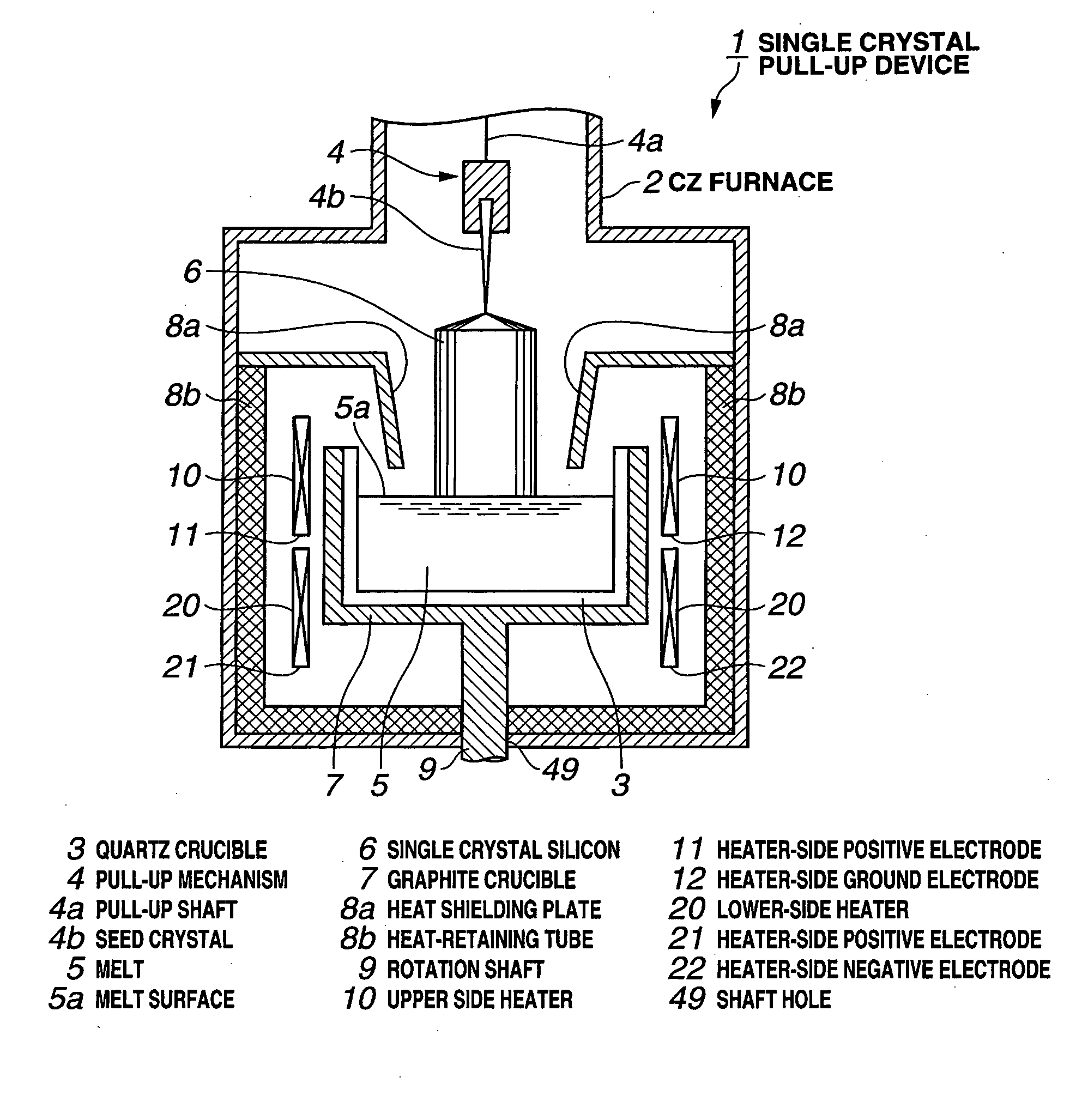
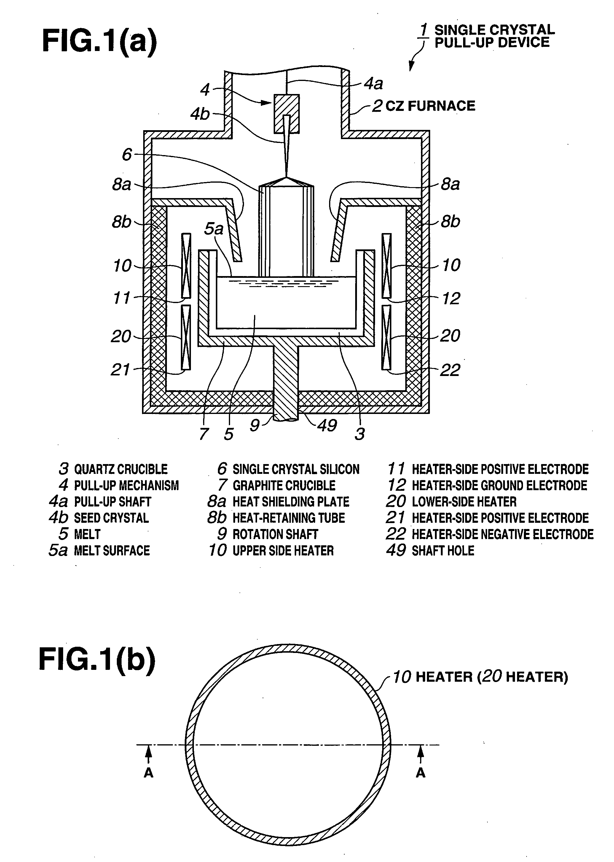
[0085]FIG. 1(a) shows a sectional view of a side of a structure of a single crystal pull-up device 1 of an embodiment. Heaters of the embodiment are incorporated into the single crystal pull-up device 1.

[0086]As shown in FIG. 1, the single crystal pull-up device 1 of the embodiment is provided with a CZ furnace (chamber) 2 as a single crystal pulling vessel.

[0087]The CZ furnace 2 has therein a quartz crucible 3 in which a material for polycrystalline silicon is melted and stored as a melt 5. The quartz crucible 3 has its exterior covered with a graphite crucible 7. An upper side heater 10 and a lower side heater 20 are provided to surround the crucibles 3, 7 to heat and melt the polycrystalline silicon material in the quartz crucible 3. The upper side heater 10 and the lower side heater 20 are vertically arran...


PUM


Abstract

An upper side heater 10 is configured so that a current passage width becomes larger at a heater lower part than at a heater upper part. Thus, the upper side heater 10 has a current-carrying cross-sectional area which becomes larger at the heater lower part than at the heater upper part, a resistance value becomes accordingly smaller at the heater lower part than at the heater upper part, and a heat generation amount becomes relatively smaller at the heater lower part than at the heater upper part. Meanwhile, a lower side heater 20 is configured so that the current passage width becomes larger at the heater upper part than at the heater lower part. Thus, the current-carrying cross-sectional area of the lower side heater 20 becomes larger at the heater upper part than at the heater lower part, a resistance value becomes accordingly smaller at the heater upper part than at the heater lower part, and a heat generation amount becomes relatively smaller at the heater upper part than at the heater lower part.

Description

TECHNICAL FIELD[0001]The present invention relates to an apparatus for manufacturing a single crystal semiconductor and a manufacturing method.BACKGROUND ART[0002]FIG. 3 shows an example of a structure of a conventional single crystal pull-up device 1.[0003]A quartz crucible 3 is disposed in a single crystal pulling vessel 2, namely a CZ furnace 2. Polycrystalline silicon (Si) is heated and melted in the quartz crucible 3. After the melting is stabilized, a single crystal silicon 6 is pulled up from a silicon melt 5 in the quartz crucible 3 by a pull-up mechanism 4 by a CZ method. When pulling up, the quartz crucible 3 is rotated by a rotation shaft 9.[0004]During a single crystal pull-up process (single batch), various types of vaporized materials are generated in the vessel 2. Accordingly, argon (Ar) gas is supplied into the single crystal pulling vessel 2 and exhausted together with the vaporized materials out of the vessel 2 to remove the vaporized materials from the vessel 2, t...

Claims


Application Information

Patent Timeline
IPC IPC(8): C30B15/14
CPCC30B15/14Y10T117/1052Y10T117/1068C30B35/00C30B29/06
Inventor IIDA, TETSUHRIOSHIRAISHI, YUTAKATOMIOKA, JUNSUKE
Owner SUMCO TECHXIV
Why Eureka
Try Eureka