

Microchip, method of manufacturing microchip, and method of detecting compositions
- Summary
- Abstract
- Description
- Claims
- Application Information
AI Technical Summary
Benefits of technology
Problems solved by technology
Method used
Image

Examples
first embodiment
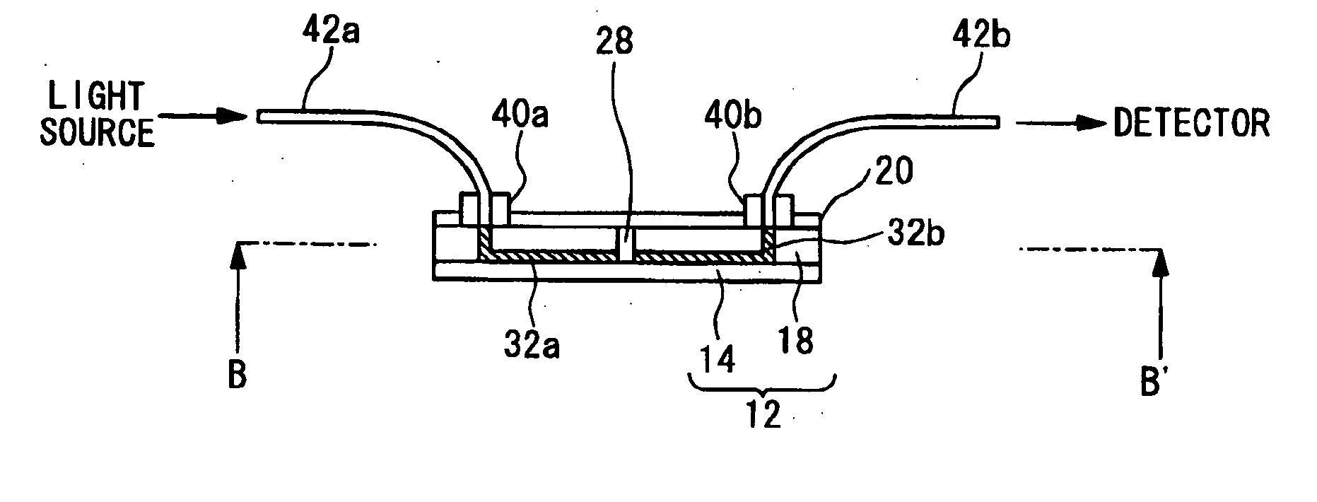
[0081]FIGS. 3A to 3C are diagrams showing structures of a microchip according to a first embodiment of the present invention. The microchip 10 according to the present embodiment has a function capable of separating compositions contained in a sample. FIG. 3A is a top view of the microchip 10. The microchip 10 is provided with a liquid reservoir 22a, a liquid reservoir 22b, a liquid reservoir 23, a liquid reservoir 24, a liquid reservoir 25a, and a liquid reservoir 25b. Also, a light leading optical fiber 42a is connected via an optical connector 40a to the microchip 10, and a light receiving optical fiber 42b is connected via an optical connector 40b to the microchip 10.
[0082]FIG. 3B is a cross sectional view of the microchip along A-A′ in FIG. 3A. The microchip 10 has a substrate 12 and a cover member 20. The substrate 12 includes a lower clad layer 14, and an upper clad layer 18 which is provided on the lower clad layer 14. A light leading optical waveguide 32a and a light recei...
second embodiment
[0111]FIG. 5 is a cross sectional view showing a structure of a microchip according to a second embodiment of the present invention. In the present embodiment, the same reference numerals in the first embodiment shown in FIG. 3C are given to the same components, and explanations thereof are properly omitted.
[0112] When a light which is transmitted from the external light source via the light leading optical waveguide 32a is entered to the separation channel 28, the entered light is broadened and scattered within the separation channel 28. In this case, an amount of light which is transmitted to the light receiving optical waveguide 32b is decreased. Therefore, according to the present embodiment, the light leading optical waveguide 32a and the light receiving optical waveguide 32b are formed in such a manner that these optical waveguides 32a and 32b have wide width portions at boundaries with respect to the separation channel 28. The wide width portions are made wider than the othe...
third embodiment
[0114]FIG. 6A is a schematic diagram for showing a microchip according to a third embodiment of the present invention. FIG. 6B is a cross sectional view showing the microchip in FIG. 6A. In the present embodiment, the same reference numerals in the first embodiment shown in FIGS. 3A and 3C are given to the same components, and explanations thereof are properly omitted.
[0115] According to the present embodiment, a microchip 52 is different from the first embodiment in that the microchip 52 has not only a combination of a light leading optical waveguide 32a and a light receiving optical waveguide 32b but also a combination of a light leading optical waveguide 34a and a light receiving optical waveguide 34b. The light leading optical waveguide 32a and the light receiving optical waveguide 32b are provided opposite to each other on both sides of the separation channel 28. Also, the light leading optical waveguide 34a and the light receiving optical waveguide 34b are provided opposite t...
PUM
 Abstract
Description
Claims
Application Information