Process of forming silicon-based nanowires

a technology of nanowires and silicon, applied in the direction of crystal growth process, polycrystalline material growth, chemistry apparatus and processes, etc., can solve the problems of large production of nano materials, difficult release of nanostructure, and high equipment and complex processes, and achieve the effect of low cos

Inactive Publication Date: 2005-08-11
IND TECH RES INST
View PDF4 Cites 52 Cited by
  • Summary
  • Abstract
  • Description
  • Claims
  • Application Information

AI Technical Summary

Benefits of technology

[0008] The invention provides a process of forming silicon-based nanowires with low cost. High-surface-oxygen-content Si powders are heated in the vacuum. The reaction gas is charged to react with the Si powder

Problems solved by technology

Usually, expensive equipment and complex processes are required, particularly for one-dimensional or two dimensional material having special shapes, which makes the massive production of the nano material difficult.
However, there are some problems occurring in the template auxiliary growth, such as the exclusive template producing method, the need of post treatments such as heat treatment, easy bonding of the nano structure

Method used


Image

  • Process of forming silicon-based nanowires
  • Process of forming silicon-based nanowires
  • Process of forming silicon-based nanowires

Examples


first embodiment

[0023]FIG. 3 is a photo illustrating fur-like silicon carbide nanowires obtained in the invention. As illustrated, it proves that massive production of silicon carbide nanowires can be achieved with low cost according to the process of the invention. FIG. 4 is a photo taken by a scanning electronic microscope (SEM). This photo clearly shows the structure of the nanowires obtained by the invention. FIG. 5 shows results of analyzing the nanowires of the invention by using an energy dispersive x-ray (EDX). As shown in FIG. 5, the nanowires consist of carbon and silicon. Since a specimen needs to coat conductive material such as gold and platinum before being analyzed, the conductive material may be found in the analysis.

second embodiment

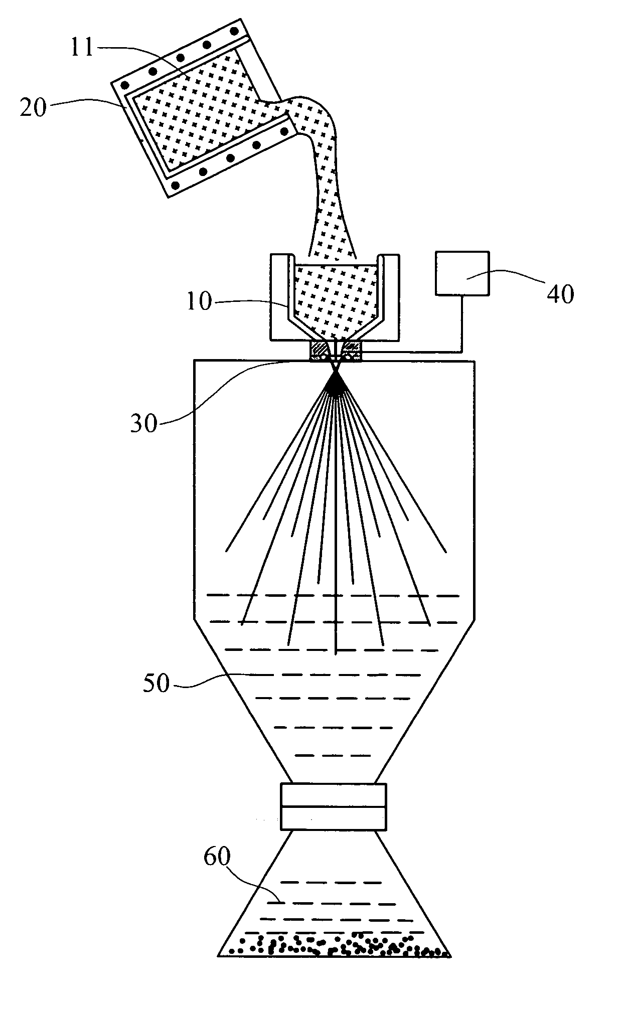
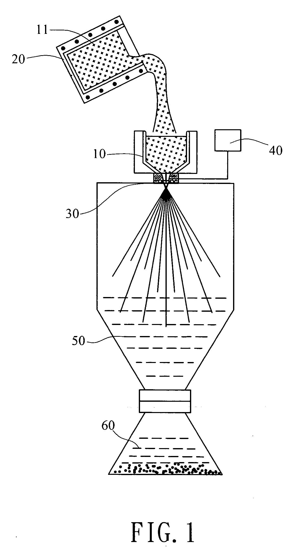
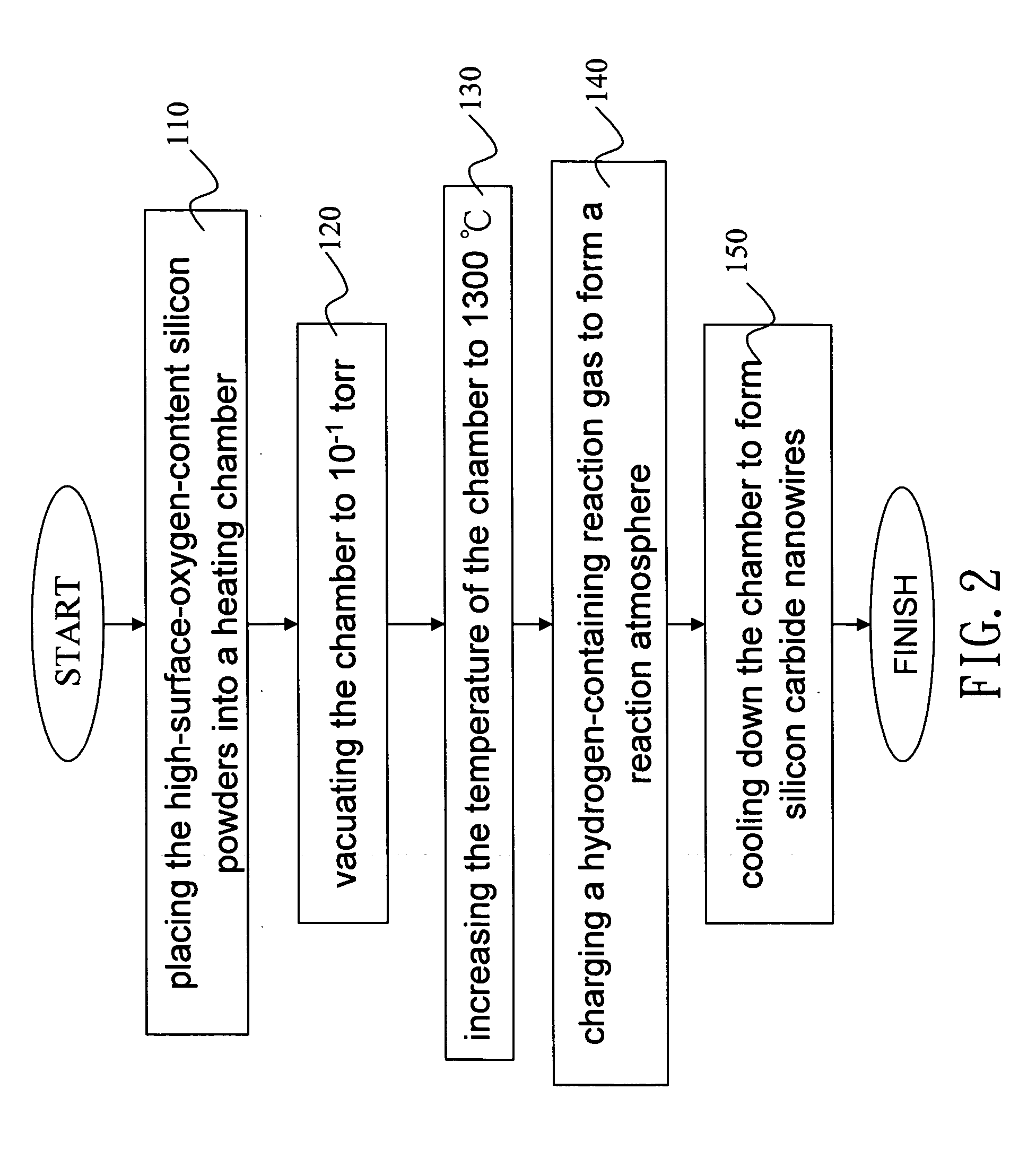
[0024] The reaction gas can be varied to generate different silicon-based nanowires. In the invention, 20 g high-surface-oxygen-content silicon powders are placed in the heating chamber. After the heating chamber is vacuated to 10−1-torr, the temperature of the heating chamber increases up to 1250° C. 90% argon and 10% mixed gas of hydrogen and nitrogen are used as the reaction gas. The atmosphere in the chamber is up to 30 to 100 torr. The temperature decreases to obtain a plurality of fur-like nanowires.

[0025]FIG. 6 is a SEM photo of nanowires obtained in a second embodiment of the invention. This photo clearly shows the structure of the nanowires obtained by this embodiment. FIG. 7 shows the results of analyzing the nanowires of the second embodiment by using an energy dispersive x-ray (EDX). As illustrated, the nanowires consist of silicon.

[0026] Furthermore, nanowires obtained by the invention can be further made into a two-dimensional structure. The high-surface-oxygen-conten...


PUM


Abstract

A process of forming silicon-based nanowires heats high-surface-oxygen-content silicon powders to initiate vapor-solid reaction to form nanowires. The reaction gas is charged to react with the Si powders to form the silicon-based nanowires such as silicon nanowires or SiC nanowires. With control of the reaction gas, the components of the nanowires can be exactly controlled without the addition of metallic catalysts. Thereby, the nanowires can be made with reduced cost.

Description

BACKGROUND OF THE INVENTION [0001] 1. Field of Invention [0002] The present invention relates to a process of forming silicon-based nanowires, and more particularly to a process of forming silicon-base nanowires in mass production. [0003] 2. Related Art [0004] When the structural dimension of material is reduced to a nanometer (nano) scale, most of the atoms locate at the surface of the material, which provides a special surface effect, volume effect and quantum effect, and the optical, thermal, electric, magnetic and mechanic properties of the material change significantly. The nano material includes nano powders, nano wires, nano films, and nano blocks. Various processes of forming the above nano material have been proposed. Usually, expensive equipment and complex processes are required, particularly for one-dimensional or two dimensional material having special shapes, which makes the massive production of the nano material difficult. [0005] For the nanowires as examples, templa...

Claims


Application Information

Patent Timeline
IPC IPC(8): C30B23/00C30B29/06C30B29/60H01L21/26
CPCC30B23/00C30B29/605C30B29/06
Inventor LAI, MING-SHYONGLIN, CHIH-JENCHEN, HUNG-CHENGWEN, JYH-CHUNG
Owner IND TECH RES INST
Why Eureka
Try Eureka