
Semiconductor wafer grinder

a technology of semiconductor devices and grinders, which is applied in the direction of grinding drives, grinding drives, manufacturing tools, etc., can solve the problems of reducing the accuracy of the grinding process, prior art machines do not incorporate dressing stations on the rotary index table, and cannot be used in a clean-room environment, so as to achieve vibration-free operation and enhance stability. the effect of the grinder

Inactive Publication Date: 2005-08-11
GERBER ROBERT
View PDF18 Cites 28 Cited by
  • Summary
  • Abstract
  • Description
  • Claims
  • Application Information

AI Technical Summary

Benefits of technology

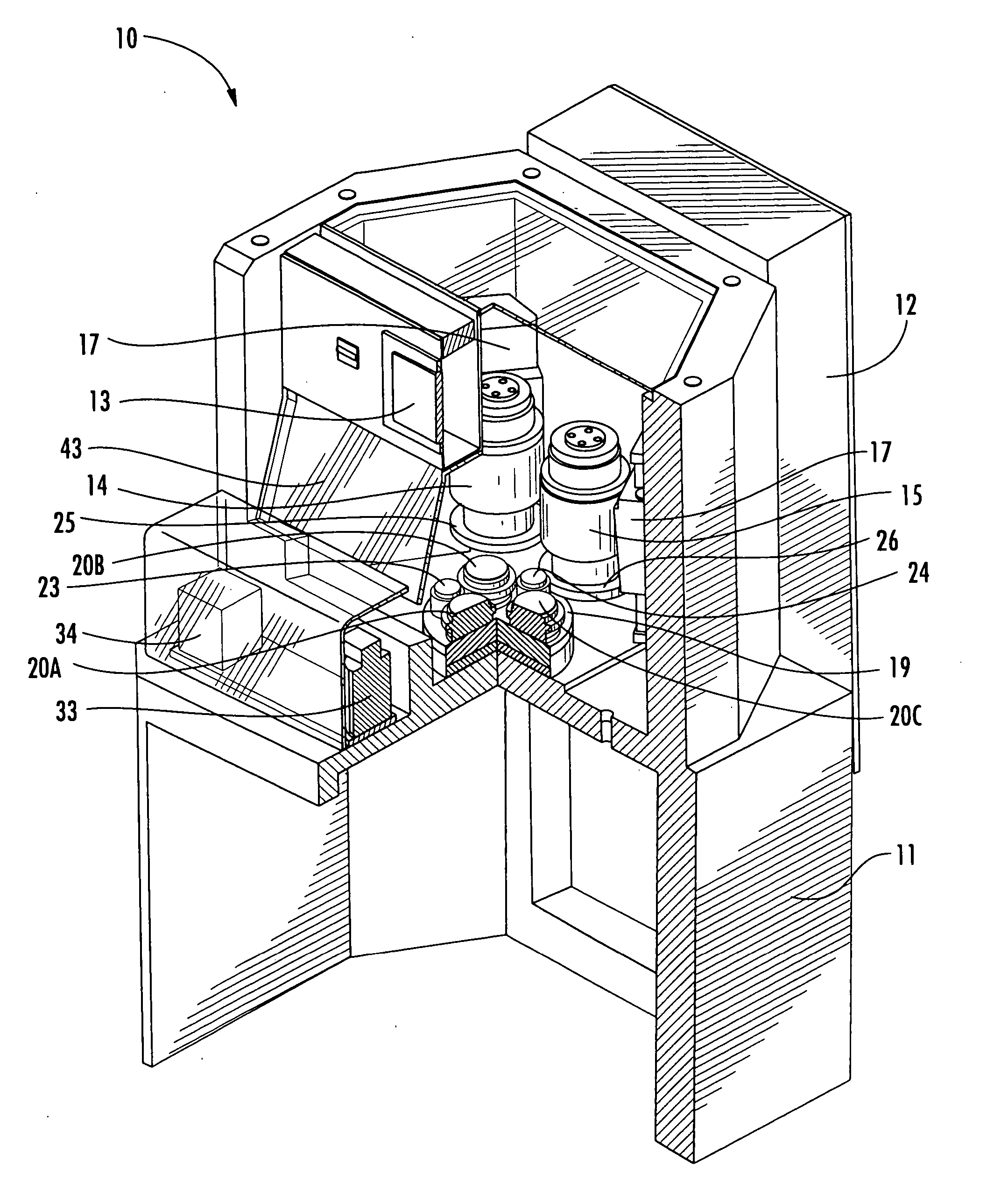
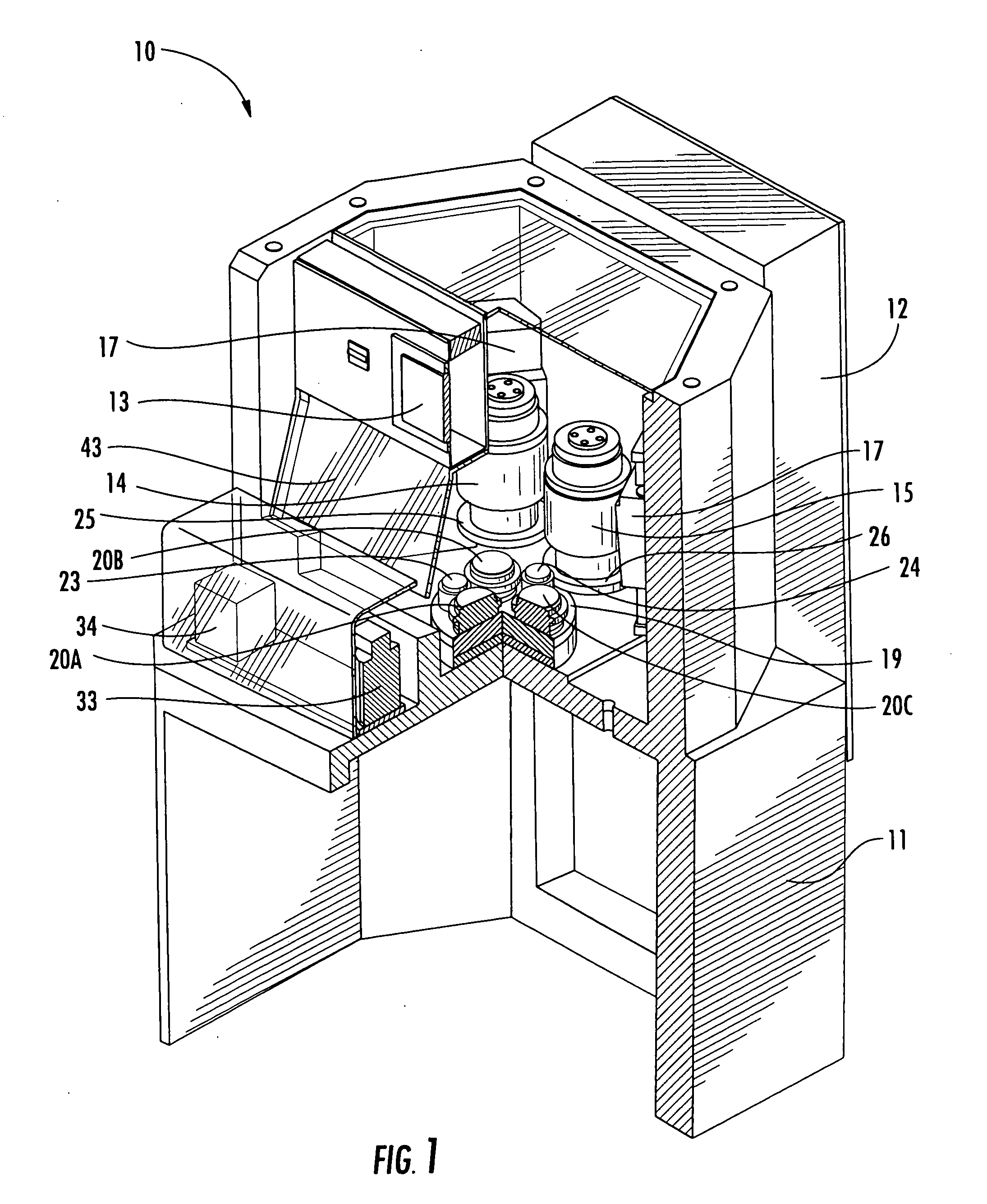
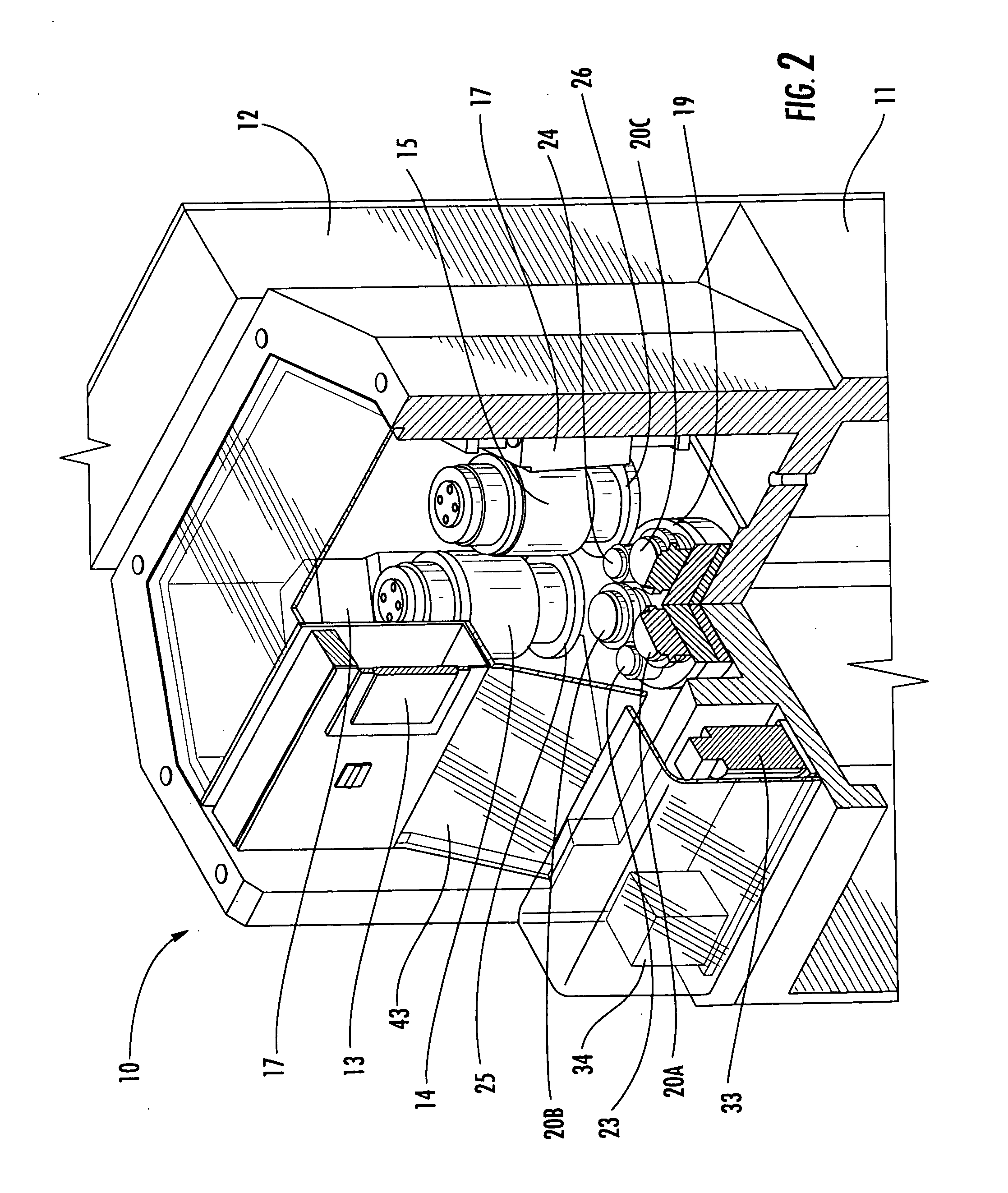
[0016] According to another preferred embodiment of the invention, the base comprises a vibration absorbing material for providing enhanced stability and vibration-free operation of the grinder during wafer grinding.
[0017] According to another preferred embodiment of the invention, the vibration material includes a polymer for preventing the base from expanding with temperature changes and allowing the base to be anchored to a surface.

Problems solved by technology

Typically, grinding machines are not capable of being used in a clean-room environment.
This is due to the fact that these machines are too big and contain other integrated features such as wash stations.
Additionally, prior art machines do not incorporate dressing stations on the rotary index table.
This can cause alignment problems for the grinding wheels, diminishing the accuracy of the grinding process.
This also results in lost time, as the grinding process is completely halted to allow the grinding wheels to rotate to the dressing station and then rotate back into position to continue grinding.

Method used


Image

  • Semiconductor wafer grinder
  • Semiconductor wafer grinder
  • Semiconductor wafer grinder

Examples


first embodiment

[0054] Referring to FIGS. 7, 8, 9, 10, 11, 12, and 13, a robotic arm type wafer handler 28 is used to bring fresh wafers to the index table 19 and remove the finished wafers from the index table 19 during the grinding process. In the invention, the wafer handler 28 is mounted for both linear and rotary movement. In this embodiment, the wafer handler is mounted to a base 29 which is slidably mounted to two rails 30 and 31 for linear motion in the horizontal plane. The two rails 30 and 31 are mounted inside of a channel 32 which has a wafer cassette 33 and 34 fixedly mounted on each end and a slot 36 cut in the center to allow linear movement of the wafer handler 28. A motor 37 is connected to the base 29 and provides the linear motion necessary for the base 29 to slide along the two rails 30 and 31. The motor 37 is capable of moving the base 29 in a back and forth motion along the two rails 30 and 31 allowing the wafer handler 28 to slide from one end of the channel 32 to the other e...

second embodiment

[0056] Referring to FIGS. 14, 15, and 16, in the invention, the robotic type wafer handler 128 is mounted for rotary motion only. In this embodiment, the wafer cassettes 133 and 134 are mounted for linear motion instead of the wafer handler 128. As above, the wafer handler 128 has a horizontal arm 138 mounted to a vertical shaft 139 which is rotated 180 degrees by a step motor 140. The arm 138 is equipped with a suction cup 142 and proximity sensors and is fully automated.

[0057] A commercially available wafer thickness measuring device, such as those produced by SigmaTech is used to measure the thickness of the wafer during the grinding process. The device uses an airflow sensor positioned above the target and allows for an exact in-process measurement of the wafer thickness in a wet environment.

[0058] Referring to FIGS. 1, 13, 16, and 17, the process for grinding a wafer includes several steps. The process starts with wafer handling. A grinding chamber gate 43 is opened to allow t...


PUM


Abstract

A grinder designed to provide an automatic grinding operation for the manufacture of a semiconductor device wafer. The grinder includes a base, a rotatable index table mounted to the base, and a grinding wheel assembly including a grinding wheel for grinding a flat surface on the wafer. The index table includes a wafer holder for receiving and holding the wafer and a dressing element for dressing the grinding wheel. The index table is selectively rotatable between a grinding position where the wafer is ground by the grinding wheel and a dressing position where the grinding wheel is dressed by the dressing element.

Description

[0001] This application claims the benefit of Provisional Application No. 60 / 542,199 filed on Feb. 5, 2004.TECHNICAL FIELD AND BACKGROUND OF THE INVENTION [0002] This invention relates to a grinding machine and a method for grinding a semiconductor device wafer. The grinding machine is designed to provide an automatic grinding operation for the manufacture of a semiconductor device wafer. More specifically, the grinding machine incorporates several automatic functions to aid in the grinding of a wafer, such as a rotary index table with dressing stations located thereon and an automatic loading and unloading device. [0003] Wafer grinding machines are well-known in the art, however, prior art designs have several disadvantages which the present invention addresses. Typically, grinding machines are not capable of being used in a clean-room environment. This is due to the fact that these machines are too big and contain other integrated features such as wash stations. The present invent...

Claims


Application Information

Patent Timeline
Patent Type & Authority Applications(United States)
IPC IPC(8): B24B7/22B24B53/02
CPCB24B53/02B24B7/228
Inventor GERBER, ROBERT
Owner GERBER ROBERT
Learn More