Corrosion-inhibiting cleaning compositions for metal layers and patterns on semiconductor substrates

a technology of metal layers and cleaning compositions, applied in the field of forming integrated circuit devices, can solve problems such as metal layer corrosion from chemical etchants

Inactive Publication Date: 2005-08-11
SAMSUNG ELECTRONICS CO LTD +1
View PDF48 Cites 51 Cited by
  • Summary
  • Abstract
  • Description
  • Claims
  • Application Information

AI Technical Summary

Problems solved by technology

Unfortunately, the use of cleaning compositions that remove residues from metal layers may lead to metal layer corrosion from chemical etchants.

Method used


Image

  • Corrosion-inhibiting cleaning compositions for metal layers and patterns on semiconductor substrates
  • Corrosion-inhibiting cleaning compositions for metal layers and patterns on semiconductor substrates
  • Corrosion-inhibiting cleaning compositions for metal layers and patterns on semiconductor substrates

Examples


Embodiment Construction

[0013] The present invention now will be described more fully herein with reference to the accompanying drawings, in which preferred embodiments of the invention are shown. This invention may, however, be embodied in many different forms and should not be construed as being limited to the embodiments set forth herein; rather, these embodiments are provided so that this disclosure will be thorough and complete, and will fully convey the scope of the invention to those skilled in the art. Like reference numerals refer to like elements throughout.

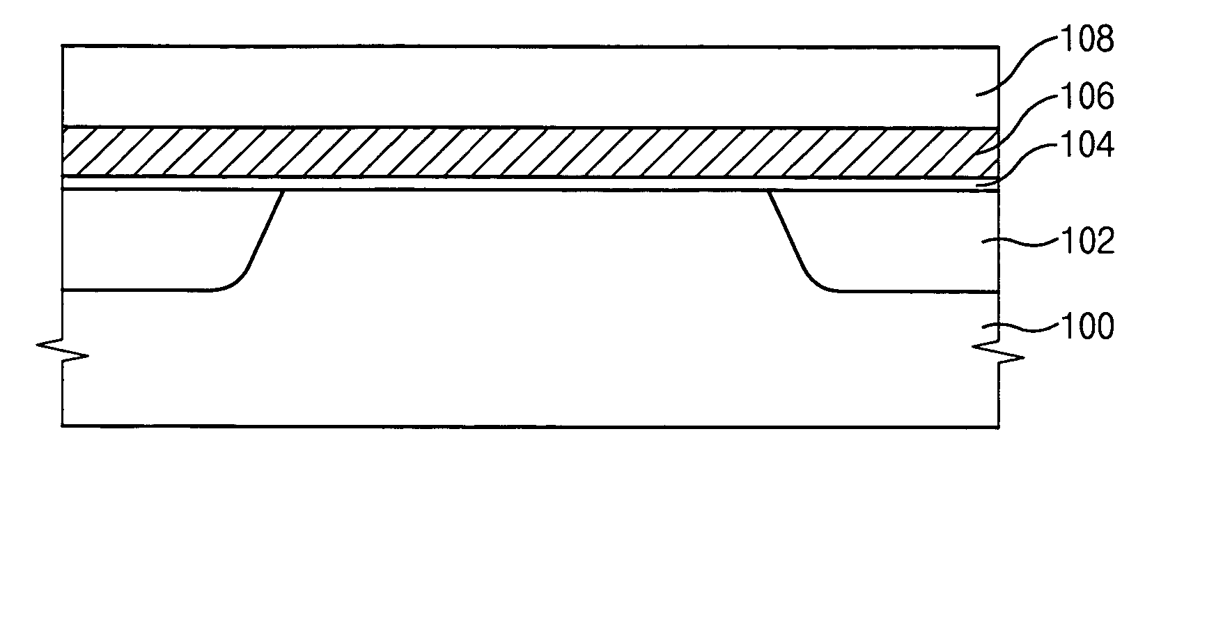
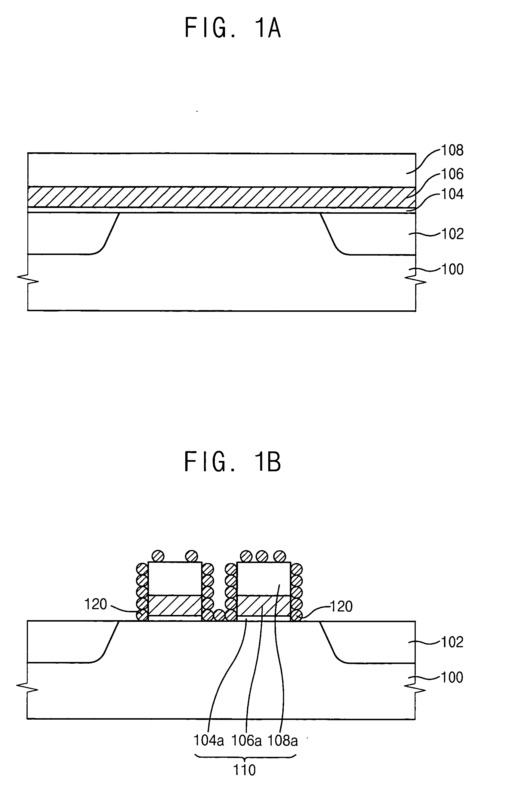
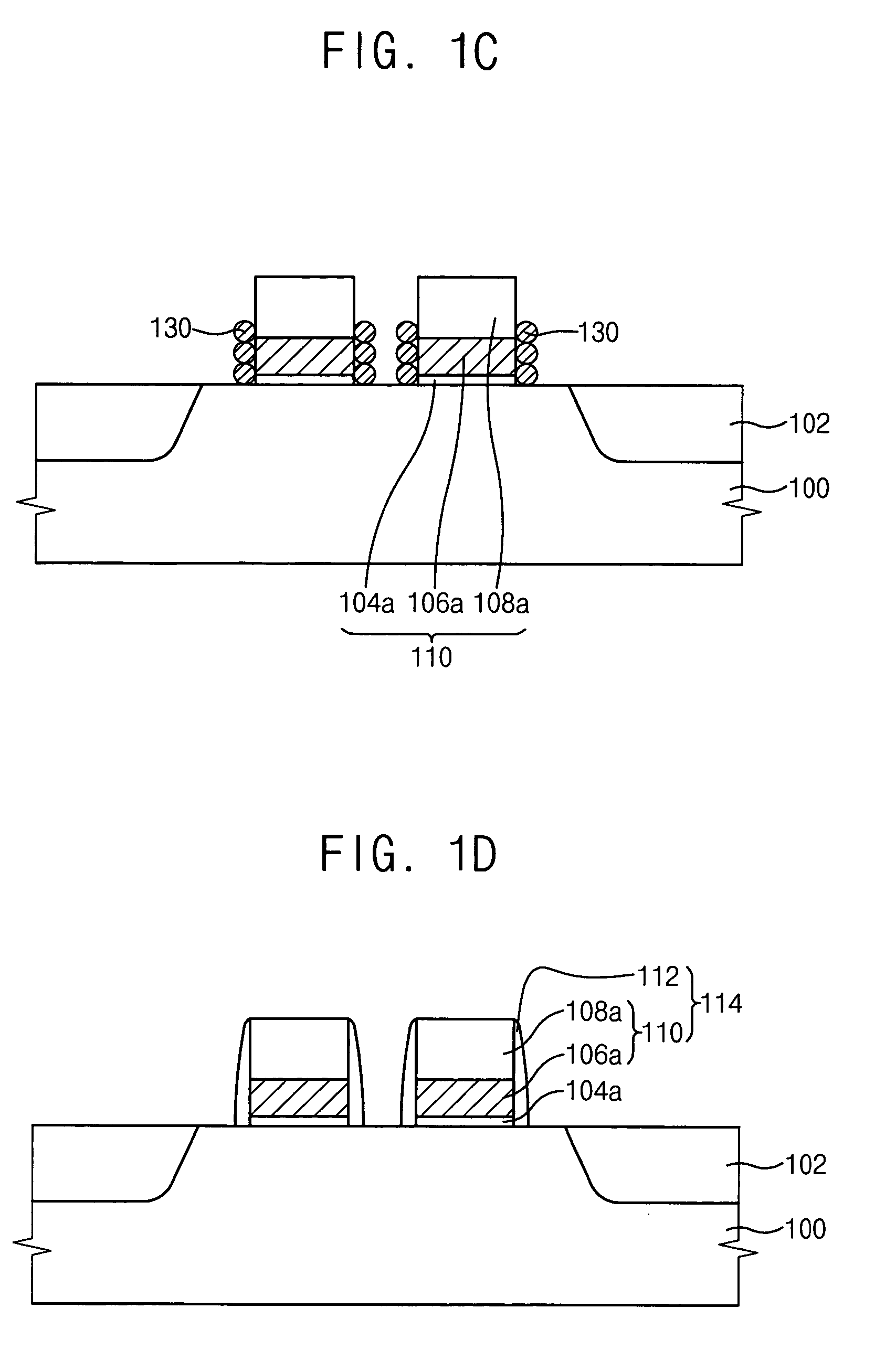
[0014] Methods of cleaning metal layers on semiconductor substrates include cleaning tungsten-based gate electrodes. As illustrated by FIG. 1A, these methods include forming a gate oxide layer 104 on a semiconductor substrate 100 having at least one semiconductor active region therein. This active region may be defined by a plurality of trench-based isolation regions 102, which may be formed using conventional shallow trench isolation (STI) t...


PUM

PropertyMeasurementUnit
corrosion-aaaaaaaaaa
resistanceaaaaaaaaaa
corrosionaaaaaaaaaa

Abstract

A corrosion-inhibiting cleaning composition for semiconductor wafer processing includes an aqueous admixture of at least water, a surfactant and a corrosion-inhibiting compound selected from a group consisting of amino phosphonates, polyamines and polycarboxylic acids. The quantity of the corrosion-inhibiting compound in the admixture is preferably in a range from about 0.0001 wt % to about 0.1 wt % and the quantity of the surfactant is preferably in a range from about 0.001 wt % to about 1.0 wt %. The aqueous admixture may also include sulfuric acid and a fluoride, which act as oxide etchants, and a peroxide, which acts as a metal etchant.

Description

REFERENCE TO PRIORITY APPLICATION [0001] This application claims priority to Korean Application Serial Nos. 2004-8798, filed Feb. 10, 2004 and 2004-35210, filed May 18, 2004, the disclosures of which are hereby incorporated herein by reference. FIELD OF THE INVENTION [0002] The present invention relates to methods of forming integrated circuit devices and, more particularly, to methods of cleaning and polishing metal layers on integrated circuit substrates. BACKGROUND OF THE INVENTION [0003] Integrated circuit chips frequently utilize multiple levels of patterned metallization and conductive plugs to provide electrical interconnects between active devices within a semiconductor substrate. To achieve low resistance interconnects, tungsten metal layers have been deposited and patterned as electrodes (e.g., gate electrodes), conductive plugs and metal wiring layers. The processing of tungsten and other metal layers frequently requires the use of cleaning compositions to remove polymer ...

Claims


Application Information

Patent Timeline
Patent Type & Authority Applications(United States)
IPC IPC(8): C09K13/04C11D1/722C09K13/08C11D1/00C11D3/02C11D3/04C11D3/20C11D3/30C11D3/36C11D3/39C11D11/00C11D17/08C23G5/036H01L21/02H01L21/28H01L21/30H01L21/302H01L21/304H01L21/321H01L21/3213H01L21/82H01L21/8239H01L21/8242H01L27/108H01L29/78
CPCC11D3/042C11D3/046C11D3/2082C11D3/30H01L21/02071C11D3/39C11D11/0047C23G1/106C11D3/364C11D3/0073C11D3/3947
Inventor LEE, KWANG-WOOKHWANG, IN-SEAKKO, YONG-SUNYOON, BYOUNG-MOONKIM, KYUNG-HYUNKIM, KY-SUBSONG, SUN-YOUNGLEE, HYUK-JINKIM, BYUNG-MOOK
Owner SAMSUNG ELECTRONICS CO LTD
Why Eureka
Try Eureka