Lithographic apparatus, interferometer and device manufacturing method

a technology of interferometer and lithographic apparatus, which is applied in the direction of electrical equipment, instruments, printing, etc., can solve the problems of measurement error and distance measurement error of interferometer, and achieve the effect of improving the accuracy of interferometric measuremen

Inactive Publication Date: 2005-08-18
ASML NETHERLANDS BV
View PDF5 Cites 14 Cited by
  • Summary
  • Abstract
  • Description
  • Claims
  • Application Information

AI Technical Summary

Benefits of technology

[0008] Embodiments of the present invention include an interferometer configured to improve accuracy of an interferometric measurement.

Problems solved by technology

Although such an interferometer provides a highly accurate measurement, measurement errors may occur due to unflatness of the measurement mirror.
Unflatness of the mirror may thus result in an error in the distance measurement by the interferometer.

Method used


Image

  • Lithographic apparatus, interferometer and device manufacturing method
  • Lithographic apparatus, interferometer and device manufacturing method
  • Lithographic apparatus, interferometer and device manufacturing method

Examples


Embodiment Construction

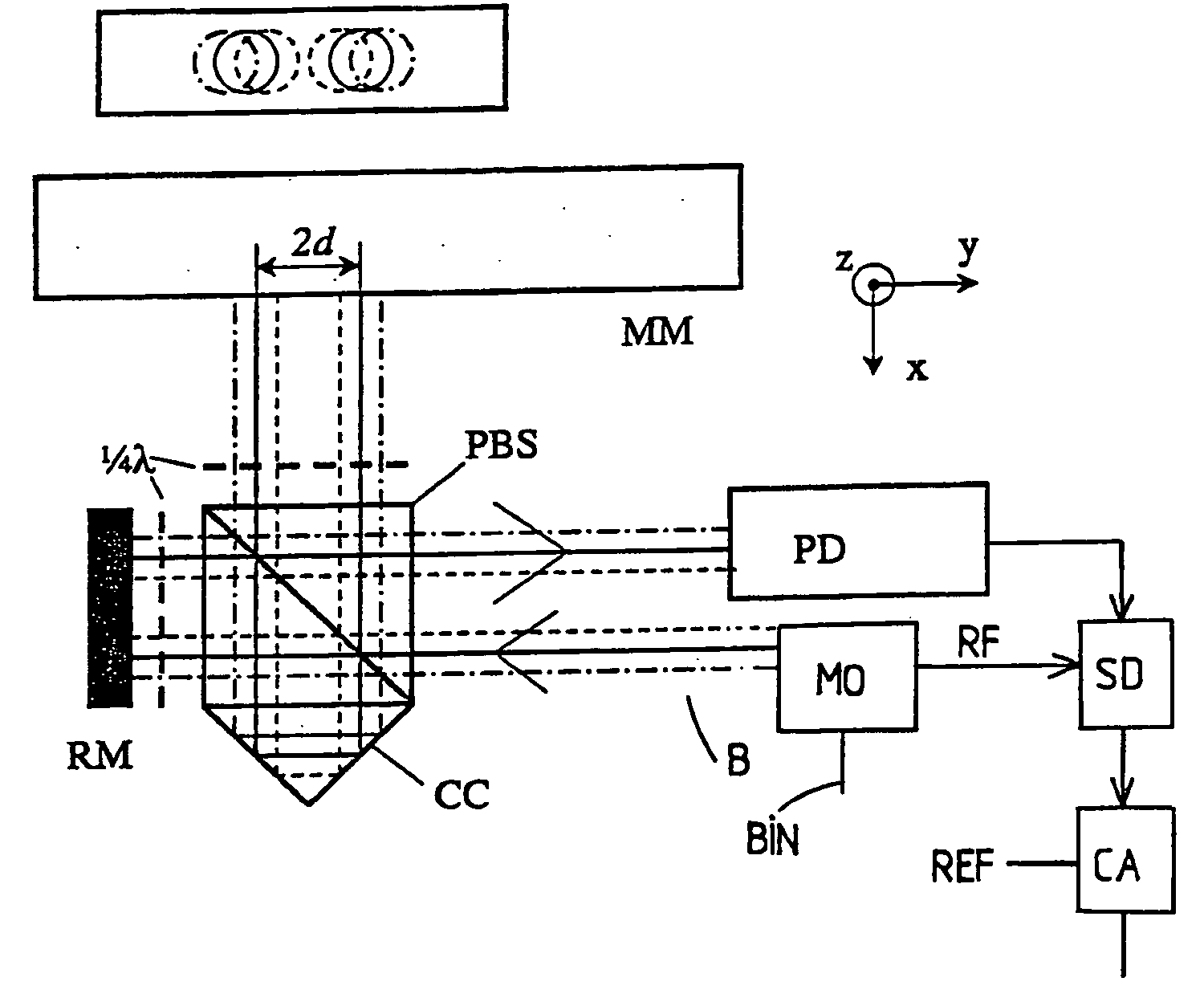
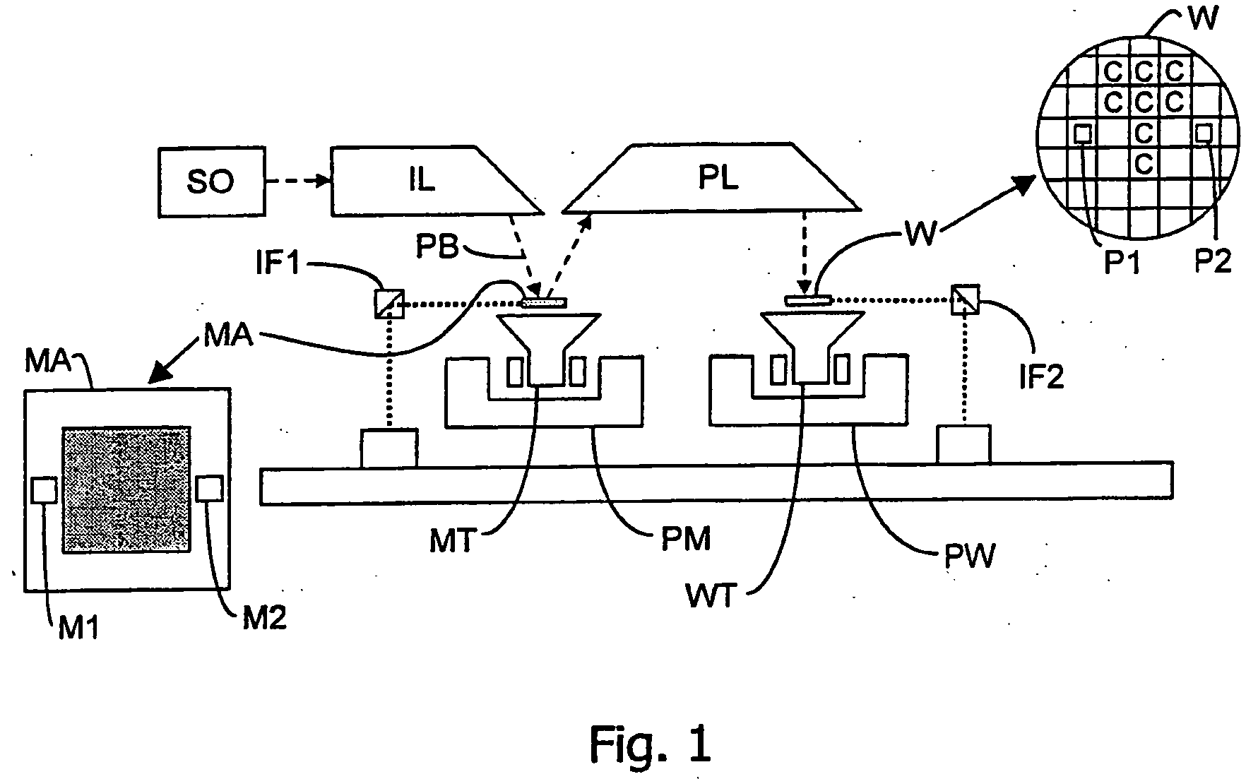
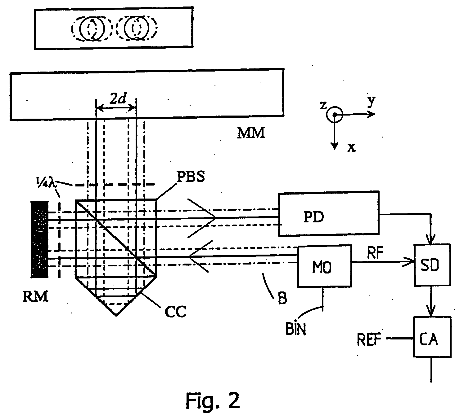
[0035]FIG. 1 schematically depicts a lithographic apparatus according to an embodiment of the invention. The apparatus includes an illumination system (illuminator) IL configured to condition a beam PB of radiation (e.g. UV or EUV radiation) and a first support structure (e.g. a mask table) MT configured to support a patterning device (e.g. a mask) MA and connected to a first positioning device PM configured to accurately position the patterning device with respect to the projection system, (“lens”), item PL. The apparatus also includes a substrate table (e.g. a wafer table) WT configured to hold a substrate (e.g. a resist-coated wafer) W and connected to a second positioning device PW configured to accurately position the substrate with respect to the projection system (“lens”), item PL; the projection system (e.g. a reflective projection lens) PL being configured to image a pattern imparted to the beam of radiation PB by patterning device MA onto a target portion C (e.g. including...


PUM

PropertyMeasurementUnit
wavelengthaaaaaaaaaa

Abstract

A lithographic apparatus includes an interferometer configured to measure a position of a mirror of the lithographic apparatus. For measuring unflatness of the mirror the interferometer includes a modulator configured to modulate a position of an input beam of the interferometer, a synchronous detector configured to synchronously detect an interfered, modulated beam, and a calculator configured to calculate an unflatness of an area of the mirror from an effect of the modulation of the position of the input beam on an output signal of the synchronous detector. The modulator can include a rotatable, tilted, plan plate.

Description

PRIORITY INFORMATION [0001] This application claims priority from European Patent Application No. 03078419.3, filed Oct. 30, 2003, the content of which is herein incorporated by reference in its entirety. BACKGROUND [0002] 1. Background of the Invention: [0003] The present invention relates to a lithographic apparatus, an interferometer and a device manufacturing method. [0004] 2. Description of Related Art: [0005] A lithographic apparatus is a machine that applies a desired pattern onto a target portion of a substrate. Lithographic apparatus can be used, for example, in the manufacture of integrated circuits (ICs). In that circumstance, a patterning device, such as a mask, may be used to generate a circuit pattern corresponding to an individual layer of the IC, and this pattern can be imaged onto a target portion (e.g. including part of, one or several dies) on a substrate (e.g. a silicon wafer) that has a layer of radiation-sensitive material (resist). In general, a single substra...

Claims


Application Information

Patent Timeline
Patent Type & Authority Applications(United States)
IPC IPC(8): G01B9/02G03F7/20G03F9/00H01L21/027
CPCG03F7/70775
Inventor PRIL, WOUTER ONNO
Owner ASML NETHERLANDS BV
Why Eureka
Try Eureka