SOI-based photonic bandgap devices

Active Publication Date: 2005-08-18
CISCO TECH INC
View PDF9 Cites 51 Cited by
  • Summary
  • Abstract
  • Description
  • Claims
  • Application Information

AI Technical Summary

Benefits of technology

[0002] The present invention relates to silicon-on-insulator (SOI)-based electro-optic devices and, more particularly, to the inclusion of photonic bandgap (PBG) structures within th

Problems solved by technology

However, both of these arrangements exhibit a relatively slow speed of operation (not acceptable

Method used


Image

  • SOI-based photonic bandgap devices
  • SOI-based photonic bandgap devices
  • SOI-based photonic bandgap devices

Examples


Example

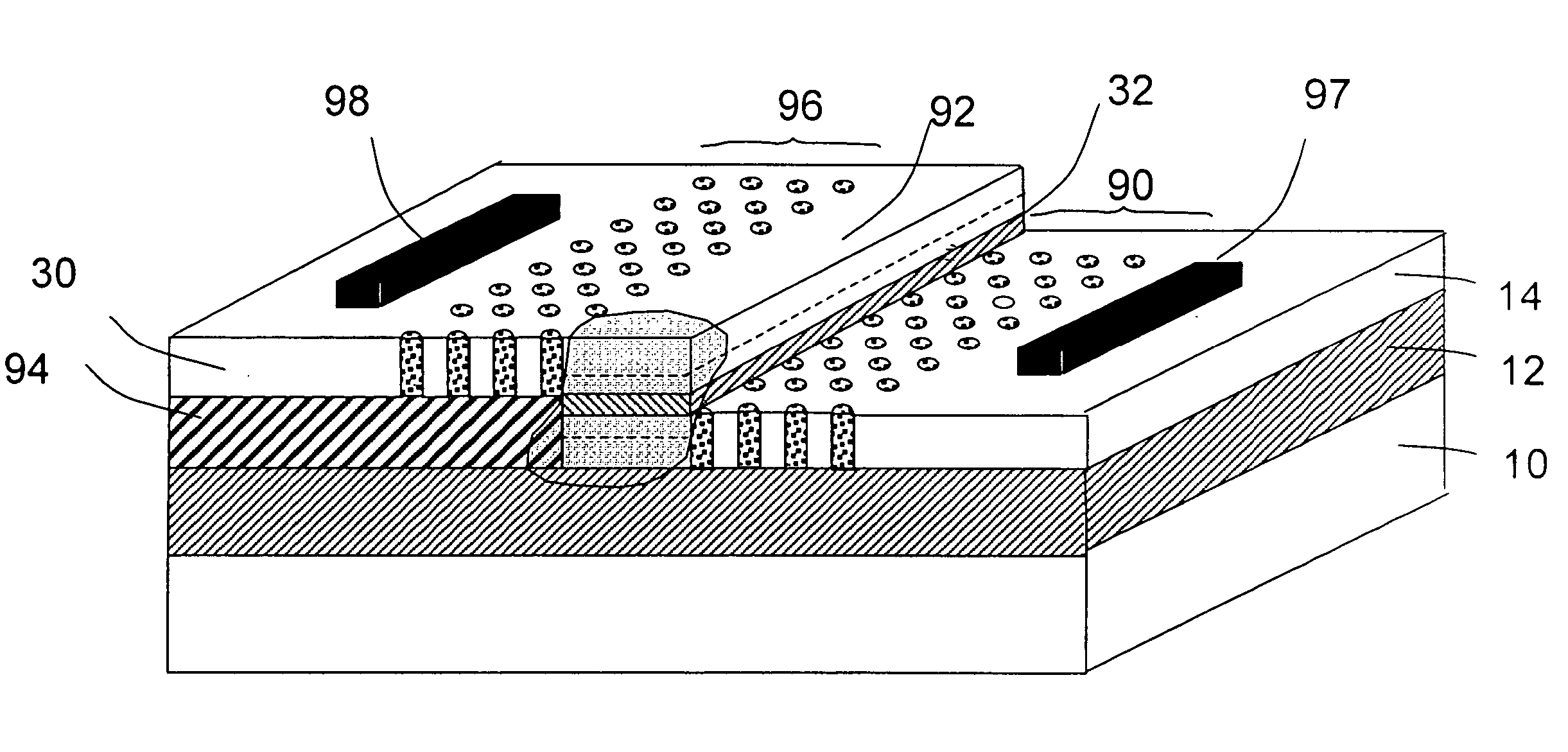
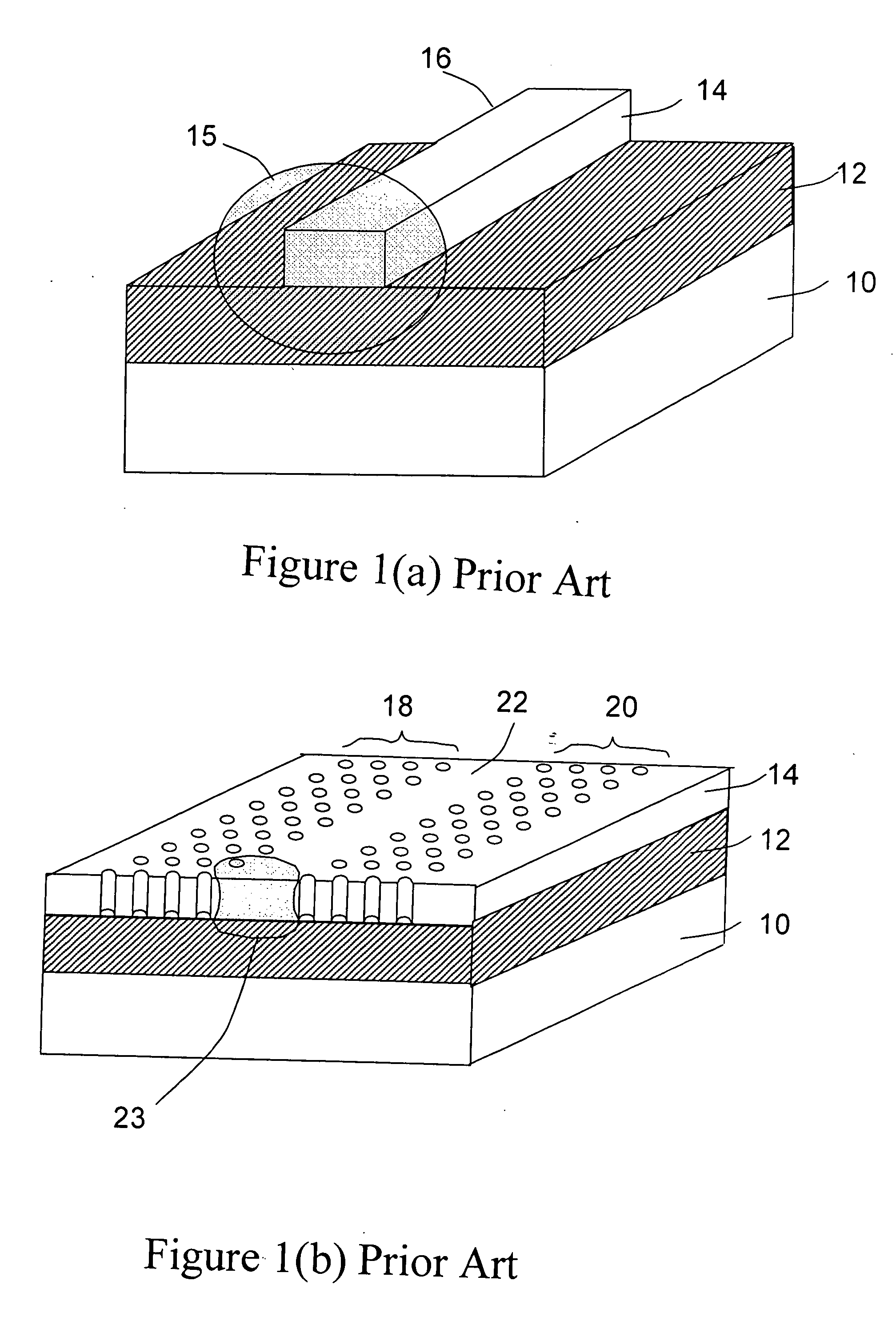
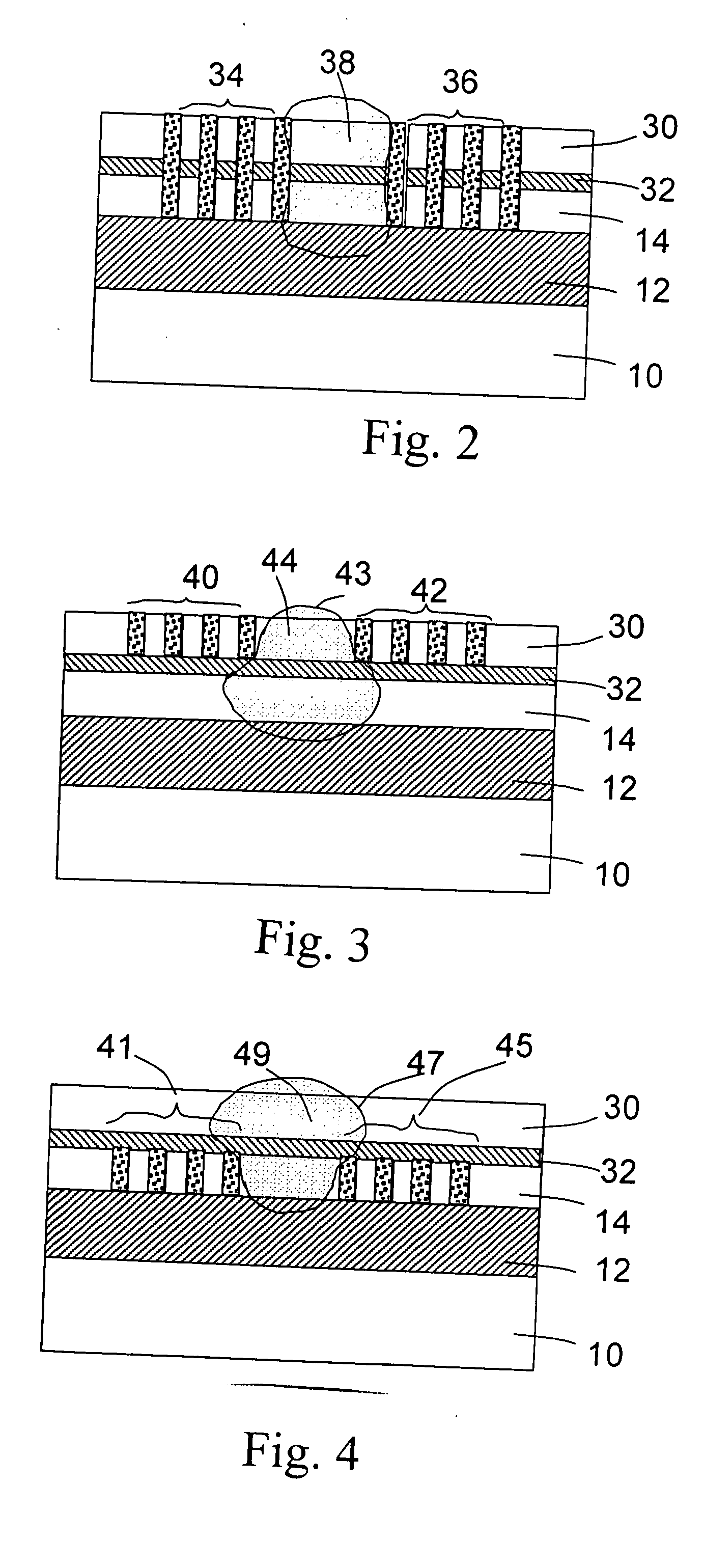
[0028] As mentioned above, the utilization of a PBG structure within an SOI-based electro-optic device results in providing relatively tight confinement of the propagating optical mode within the defined waveguide region, as opposed to prior structures where a significant amount of the optical power would reside in the evanescent tails in the cladding regions surrounding a silicon strip or rib waveguide. FIGS. 1(a) and 1(b) illustrate this aspect of an exemplary PBG structure, where FIG. 1(a) illustrates a prior art SOI structure comprising a silicon substrate 10, an insulating layer 12 and an SOI layer 14. The boundary of an optical mode 15 for a signal propagating along a strip waveguide 16 formed in SOI layer 14 is also shown. It is obvious from this depiction that a significant portion of the energy within optical mode 15 resides in the evanescent tails within insulating layer 12, as well as in the other low index materials (not shown) that surround strip waveguide 16. FIG. 1(b)...


PUM


Abstract

An SOI-based photonic bandgap (PBG) electro-optic device utilizes a patterned PBG structure to define a two-dimensional waveguide within an active waveguiding region of the SOI electro-optic device. The inclusion of the PBG columnar arrays within the SOI structure results in providing extremely tight lateral confinement of the optical mode within the waveguiding structure, thus significantly reducing the optical loss. By virtue of including the PBG structure, the associated electrical contacts may be placed in closer proximity to the active region without affecting the optical performance, thus increasing the switching speed of the electro-optic device. The overall device size, capacitance and resistance are also reduced as a consequence of using PBGs for lateral mode confinement.

Description

CROSS-REFERENCE TO RELATED APPLICATION [0001] This application claims the priority of U.S. Provisional Application No. 60 / 544,088, filed Feb. 12, 2004.SUMMARY OF THE INVENTION [0002] The present invention relates to silicon-on-insulator (SOI)-based electro-optic devices and, more particularly, to the inclusion of photonic bandgap (PBG) structures within the SOI devices to provide for improved lateral confinement of a propagating optical signal, thus reducing optical loss and improving the speed of such SOI-based electro-optic devices. BACKGROUND OF THE INVENTION [0003] Photonic bandgap (PBG) structures, which represent the optical equivalent of the energy gap in semiconductors, promise a wealth of new, very compact, optical devices. PBG structures can confine light in very tight regions, allowing for the radiation to be guided or bent around sharp corners with virtually no energy loss. PBGs are expected to reduce the size of optical devices by orders of magnitude and allow for a lar...

Claims


Application Information

Patent Timeline
IPC IPC(8): G02B26/00G02F1/00G02F1/025
CPCG02F2202/32G02F1/025
Inventor GOTHOSKAR, PRAKASHGHIRON, MARGARETMONTGOMERY, ROBERT KEITHPATEL, VIPULKUMARPATHAK, SOHAMPIEDE, DAVIDSHASTRI, KALPENDUYANUSHEFSKI, KATHERINE A.
Owner CISCO TECH INC
Why Eureka
Try Eureka