Laser beam irradiating apparatus, laser beam irradiating method, and method of manufacturing a semiconductor device

a laser beam irradiation and semiconductor technology, applied in the direction of manufacturing tools, instruments, optical elements, etc., can solve the problems of unsatisfactory irradiation of target objects, increased attenuation, and unwanted variance in a single substrate, so as to improve the durability of flexible substrates, reduce weight, and simple optical systems

Inactive Publication Date: 2005-08-18
SEMICON ENERGY LAB CO LTD
View PDF38 Cites 15 Cited by
  • Summary
  • Abstract
  • Description
  • Claims
  • Application Information

AI Technical Summary

Benefits of technology

[0023] Also, a method of irradiating a laser beam of the invention includes: emitting a plurality of laser beams respectively from a plurality of lasers, synthesizing the plurality of laser beams into a single laser beam on a target object to be irradiated and irradiating the synthesized laser beam to the target object by moving the synthesized laser beam on the target object while keeping a specific shape thereof. By keeping a constant angle of incidence, it is possible to irradiate the laser beam to the target object while keeping the specific shape thereof. Further, because reflection from the surface of the target object can be constant, uniform annealing can be achieved.
[0030] Further, in the above arrangement, as a substrate on which is formed the semiconductor film may be a glass substrate, a quartz substrate, a plastic substrate, a metal substrate, a flexible substrate, etc. The glass substrate includes substrates made of glass, such as barium borosilicate glass and aluminum borosilicate glass. The flexible substrate includes a film of substrate made of PET, PES, PEN, acrylic, etc. When a semiconductor device is manufactured using the flexible substrate, a reduction of weight can be expected. In order to improve the durability of the flexible substrate, it is preferable to provide a single- or multi-layer barrier layer, such as an aluminum film (AlON, AlN, AlO, etc.), a carbon film (DLC (diamond-like carbon), etc.), and a film of SiN on the principal surface or both on the principal surface and the back surface.
[0031] By applying the arrangements of the invention, it is possible to form a laser beam having an excellent distribution of energy density on the irradiation surface or in the vicinity thereof. Also, such a laser beam can be formed through a simple optical system. When annealing is applied to a target object using such a laser beam, uniform annealing can be achieved. Further, because the laser beam is formed by overlapping the regions including the attenuated regions, more regions have energy density suitable to annealing, and annealing can be achieved in an extremely efficient manner. For example, when a semiconductor film is annealed by such a laser beam, a semiconductor film having homogeneous physical properties can be obtained, and when TFTs are manufactured from this semiconductor film, unwanted variance in electrical characteristics can be lessened. Further, the operating characteristics and reliability of a semiconductor device incorporating these TFTs can be improved.

Problems solved by technology

However, the energy density in the edge portions of a laser beam emitted from the laser is small in comparison with that in the vicinity of the center, and there is a tendency that expanding a laser beam further through an optical system makes the attenuated region more noticeable.
The attenuated region has insufficient energy density in comparison with that at the center of a laser beam, and therefore, when a laser beam having the attenuated regions is irradiated, a target object cannot be irradiated in a satisfactory manner.
Hence, when TFTs are manufactured from such a semiconductor film, the TFTs manufactured from the portion irradiated by the attenuated regions have poor electrical characteristics, which causes unwanted variance in a single substrate.

Method used


Image

  • Laser beam irradiating apparatus, laser beam irradiating method, and method of manufacturing a semiconductor device
  • Laser beam irradiating apparatus, laser beam irradiating method, and method of manufacturing a semiconductor device
  • Laser beam irradiating apparatus, laser beam irradiating method, and method of manufacturing a semiconductor device

Examples


first embodiment

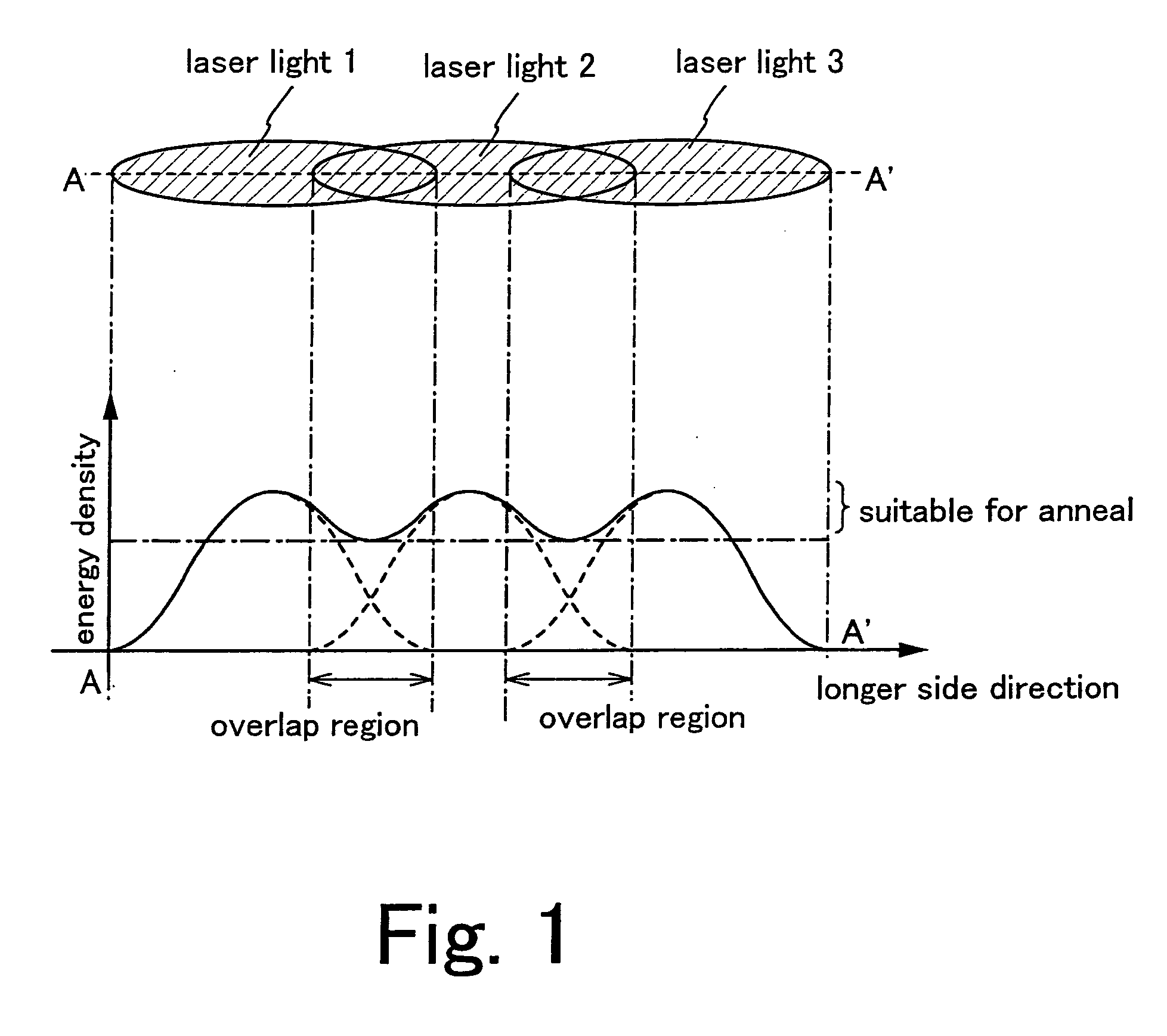
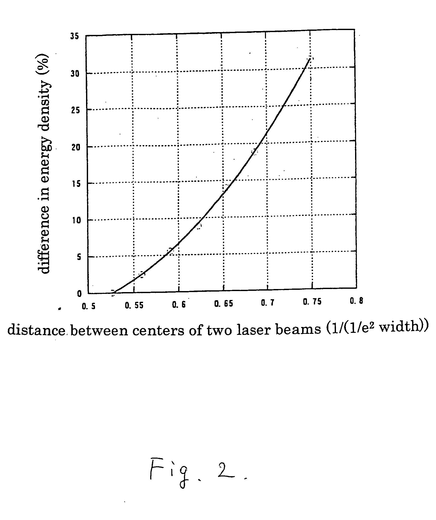
[0049] The present embodiment will describe a relation of a distance between laser beams versus the energy density shown in FIG. 1 with reference to FIG. 2, and FIG. 7.

[0050] As shown in FIG. 1, by synthesizing a plurality of laser beams at regions including the attenuated regions, it is possible to achieve uniform irradiation efficiently. Also the energy density suitable to annealing has the upper limit (line α) and the lower limit (line β), and when a difference in energy density falls within this range, uniform annealing can be achieved. However, an example in the drawings shows a case where a difference in energy density is the largest, and in practice, it is preferable to apply annealing under the condition such that reduces a difference in energy density a little. Here, given 1 as the beam width (a half width at 1 / e2) of a laser beam having a Gaussian distribution as the energy density distribution, and 100% as the average value of the peak value and the minimal value somewhe...

second embodiment

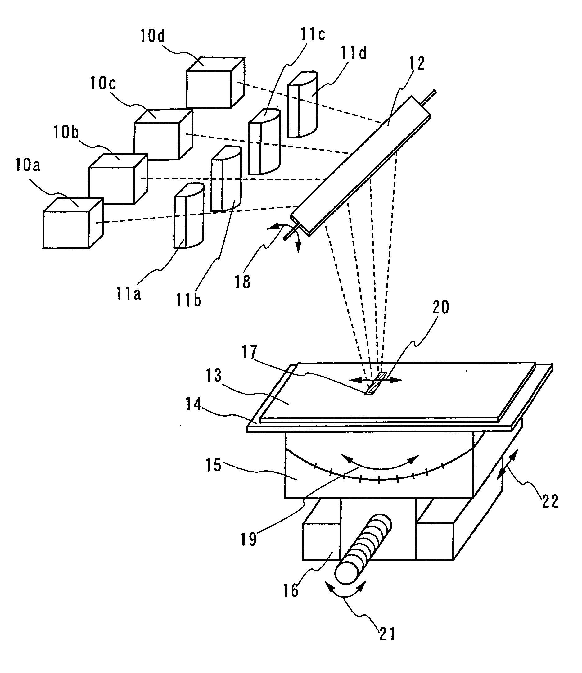
[0057] A second embodiment of the invention will now be explained with reference to FIG. 3 and FIG. 4A through FIG. 4C.

[0058] Laser beams emitted from respective lasers 10a through 10d are expanded in the longer direction by their respective convex cylindrical lenses 11a through 11d. Although it is not shown in the drawings, beam collimators for converting laser beams emitted from the respective lasers 10a through 10d into parallel beams or beam expanders for expanding or narrowing laser beams may be provided between the lasers 10a through 10d and the convex cylindrical lenses 11a through 11d. The respective laser beams are reflected by a galvanometer mirror 12 and reach a substrate 13.

[0059] When the laser beams are synthesized at their respective attenuated regions in the longer direction on the substrate 13 in this manner, a long laser beam 17 extending in the longer direction can be obtained, which is able to irradiate a target object in the same manner whether the energy dens...

third embodiment

[0069] The present embodiment will describe an optical system using a polygonal mirror 23 instead of the galvanometer mirror 12 used in the second embodiment above with reference to FIG. 5.

[0070] Laser beams emitted from respective lasers 10a through 10d are expanded in the longer direction by their respective convex cylindrical lenses 11a through 11d. Although it is not shown in the drawing, beam collimators for converting laser beams emitted from the respective lasers 10a through 10d into parallel beams or beam expanders for expanding or narrowing laser beams may be provided between the lasers 10a through 10d and the convex cylindrical lenses 11a through 11d. The respective laser beams are reflected by the polygonal mirror 23 and reach a substrate 13.

[0071] When laser beams are synthesized at their respective attenuated regions in the longer direction on the substrate 13 in this manner, a long laser beam 17 extending in the longer direction can be obtained, which is able to irra...


PUM

PropertyMeasurementUnit
aspect ratioaaaaaaaaaa
wavelengthaaaaaaaaaa
transmittanceaaaaaaaaaa

Abstract

A laser beam irradiating apparatus comprising, a plurality of lasers, member for synthesizing a plurality of laser beams emitted respectively from the plurality of lasers into a single laser beam on a stage, and member for moving the synthesized laser beam on the stage while keeping a specific shape thereof. A semiconductor film can be crystallized or an impurity element doped therein can be activated by irradiating a laser beam to the semiconductor film from the laser beam irradiating apparatus arranged as above. Consequently, it is possible to provide a laser beam irradiating apparatus capable of achieving uniform annealing efficiently by employing an optical system simpler than a conventional one and using laser beams having attenuated regions. Also, it is possible to provide a method of irradiating a laser beam using the laser beam irradiating apparatus, and to provide a method of manufacturing a semiconductor device including the laser beam irradiating method in the fabrication sequence thereof.

Description

BACKGROUND OF THE INVENTION [0001] 1. Field of the Invention [0002] The present invention relates to a method of irradiating an object as a target of irradiation (hereinafter simply referred to as the target object) through the use of a laser beam (hereinafter, referred to as laser annealing) and to a laser beam irradiating apparatus (an apparatus including a laser and an optical system for guiding a laser beam outputted from the laser to the target object) for performing the laser beam irradiating method. The invention also relates to a method of manufacturing a semiconductor device manufactured through the fabrication sequence including the laser beam irradiating method. The semiconductor device referred to herein means general devices designed to function by exploiting the semiconductor characteristics, and includes, for example, electro-optic devices, such as a liquid crystal display and a light emitting device, and electronic equipment incorporating the electro-optic devices as...

Claims


Application Information

Patent Timeline
Patent Type & Authority Applications(United States)
IPC IPC(8): B23K26/073G02B26/10H01L21/20H01L21/268H01L21/28H01L21/336H01L21/77H01L21/84H01L27/12H01L29/786
CPCB23K26/0604B23K26/0608B23K26/073B23K26/0738B23K26/0807B23K26/0815H01L27/1285B23K2201/40H01L21/2026H01L21/268H01L27/12H01L29/66757B23K26/0823B23K26/0821B23K26/082B23K2101/40H01L21/02683H01L21/02422H01L21/02502H01L21/02488H01L21/0242H01L21/02672H01L21/02425H01L21/02686H01L21/02678H01L21/02532H01L21/02381H01L21/02691H01L21/02675
Inventor TANAKA, KOICHIRO
Owner SEMICON ENERGY LAB CO LTD
Why Eureka
Try Eureka