Integrated circuit inductane and the fabrication method thereof

a technology of integrated circuits and inductances, which is applied in the direction of inductances, semiconductor/solid-state device details, semiconductor devices, etc., can solve the problems of complex manufacturing process, high cost, and inability to manufacture, and achieve low cost, good performance, and simple production process

Active Publication Date: 2005-08-18
ADVANCED SEMICON ENG INC
View PDF2 Cites 6 Cited by
  • Summary
  • Abstract
  • Description
  • Claims
  • Application Information

AI Technical Summary

Benefits of technology

[0011] Comparing the effect of the method of the present invention with the one of the prior art, the manufacture process provided by the present invention can fabricate an integrated circuit inductance having a simple production process, low cost, a near equal loop size and good performance, due to making the order of the planarization processes of the inductance loops substantially perpendicular to the wafer and the direction of the current of the inductance substantially in parallel with the wafer, by way of the manufacture process of the plugs and the conductive wires of the integrated-circuit process.

Problems solved by technology

The most part of the circuit components, such as transistors, could still have good performances after being micro-miniaturized into the plane structures via the integrated circuit process, but some of the circuit components, especially the inductance that essentially must be a three-dimension structure, could not.
As far as the manufacture process of the inductance is concerned, apparently, utilizing the photolithography process with a lot of masks to stack the loops of the inductance layer by layer upward is needed, and that makes the manufacture process become complicated and have a higher cost.

Method used


Image

  • Integrated circuit inductane and the fabrication method thereof
  • Integrated circuit inductane and the fabrication method thereof
  • Integrated circuit inductane and the fabrication method thereof

Examples


Embodiment Construction

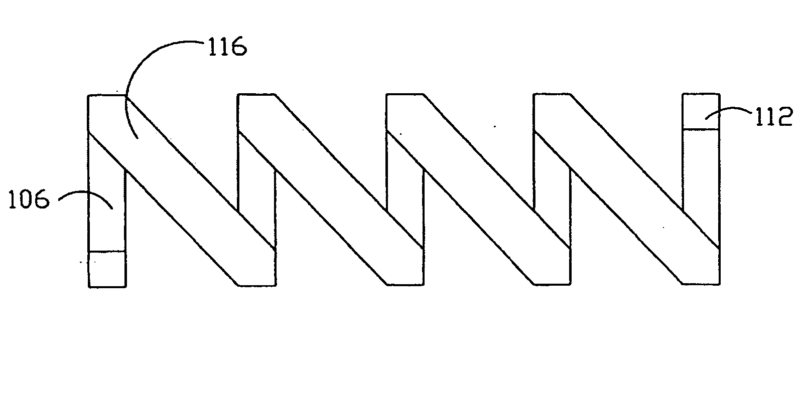
[0041] It is necessary to notice that the manufacture processes and the structures described below do not include the complete ones. The present invention can be implemented by any kind of manufacturing technologies, and only the necessary manufacturing technologies promoting to understand are described in the following. The invention will be explained in detail in accordance with the accompanying drawings. It is necessary to illustrate that the drawings in the below are only in simplified forms and not drawn in proportion to the real cases. Further, the dimensions of the drawings are enlarged for explaining and understanding more clearly.

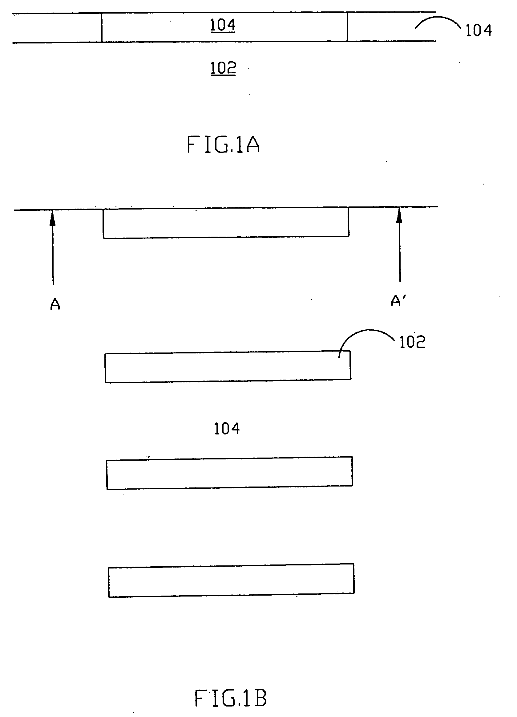
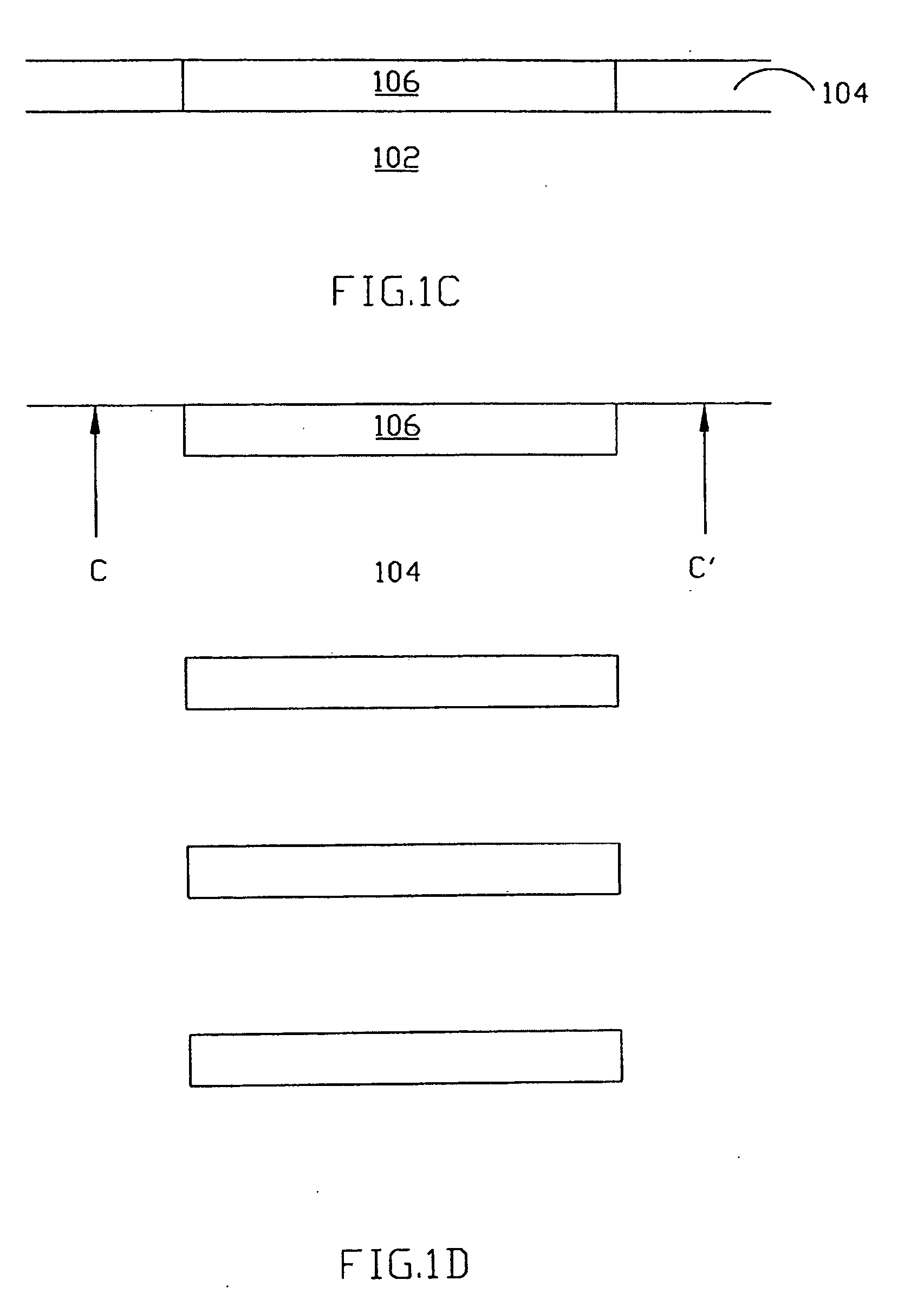
[0042] In one embodiment of the present invention, an integrated circuit inductance is formed with the integrated-circuit process. Referring to FIG. 1A, a dielectric layer 102 and a photo-resist layer 104 thereon are provided, and a first pattern is formed in the photo-resist layer 104 by a photolithography process. The substrate under the dielect...


PUM


Abstract

An integrated circuit inductance and the fabrication method thereof are disclosed. The manufacture process provided by the present invention fabricates an integrated circuit inductance having a simple production process, low cost, a near equal loop size and good performance, due to making the order of the planarization processes of the inductance loops substantially perpendicular to the wafer and the direction of the current of the inductance substantially in parallel with the wafer, by way of the manufacture process of the plugs and the conductive wires of the integrated-circuit process.

Description

BACKGROUND OF THE INVENTION [0001] 1. Field of the Invention [0002] The present invention relates to an inductance and a fabrication method thereof, and more particularly to an integrated circuit inductance and a fabrication method thereof. [0003] 2. Description of the Prior Art [0004] It can be said that the invention of the integrated circuit has more influence on the development of the human culture than the invention of the steam engine and the industrial revolution did during the last forty years since the integrated circuit was invented in 1985. In 1946, the University of Pennsylvania had carried out a first vacuum-tube electronic digital computer called an electronic numerical integrator and calculator (ENIAC). The computer was the first calculating machine composed of electronic devices, 1800 vacuum tubes, could operate 5000 times addition operation per minute. Comparing the operation velocity of ENIAC with the recent central processing unit (CPU) whose velocity even can rea...

Claims


Application Information

Patent Timeline
Patent Type & Authority Applications(United States)
IPC IPC(8): H01L21/02H01L21/8222H01L23/522H01L27/04
CPCH01L23/5227H01L28/10H01L2924/0002H01L2924/00
Inventor HUANG, MIN-LUNG
Owner ADVANCED SEMICON ENG INC
Why Eureka
Try Eureka