Method for aligning capacitor plates in a security tag and a capacitor formed thereby

a technology of security tags and capacitor plates, applied in capacitor manufacture, fixed capacitor details, instruments, etc., can solve the problems of limiting the number of different kinds of materials that can be used to form substrates, the cost of the substrate itself and the design limitations placed on the tag, and the inability to fabricate the elements of the lc-based tag

Inactive Publication Date: 2005-08-25
CHECKPOINT SYST INC
View PDF85 Cites 44 Cited by
  • Summary
  • Abstract
  • Description
  • Claims
  • Application Information

AI Technical Summary

Benefits of technology

[0059]FIG. 11 is a schematic representation of a color printing press and security tag fabrication system for applying colored ink patterns and circuit elements to the surfaces of a substrate in accordance with the system and method of the present invention;
[0060]FIG. 12 is a schematic representation of an input stage of a security tag fabrication system for applying circuit elements to a substrate in accordance with the method of the invention;
[0061]FIGS. 13A and 13B show plan and cross-sectional views, respectively, of a carrier bearing circuit elements for fabricating exemplary security tags in accordance with the system and method of the present invention;
[0062]FIG. 14 shows a schematic representation of an alternate embodiment of a fabrication system and method for fabricating exemplary security tags in accordance with the system and method of the present invention; and
[0063]FIG. 15 shows a capacitor for a security tag formed in accordance with the present invention.

Problems solved by technology

This method of fabricating the elements of an LC-based tag has several problems.
One particularly significant problem is the cost of the substrate itself and the design limitations placed on the tag by various substrate requirements.
This limits the number of different kinds of materials that can be used to form substrates.
This limits the amount of capacitance that can be provided on a unit area of substrate surface.
This factor places additional limitations on the materials that can be used in the design of substrates.
Under these circumstances, it may not be possible to optimize the dielectric properties of the substrate when selecting a dielectric material or a dielectric thickness for use as a component of a security tag.
The inability to optimize the dielectric properties of the dielectric materials results in many problems, such as increased capacitor size, lower tag yields and hence, increased costs for the fabrication of security tags.
Other problems encountered in forming the elements of an LC-based tag arise from the photo-etching process.
For example, the photo-etching process can be slow and quite expensive.
In addition to the high cost of the photo-etching process itself, the fact that the process requires environmentally unsafe chemicals creates disposal problems for the spent materials.
As will be appreciated by those skilled in the art, the procedures required to safely dispose of spent photo-etching materials significantly increase the costs of producing security tags.
Furthermore, substantial amounts of conductive material must be removed by the etching process when forming the conductor layers of the tag.
This further increases the costs of the fabrication process as a result of the waste of conductive material and / or the complications of performing various recovery processes, such as recovering aluminum, when forming the tags.
An additional area of difficulty encountered when using the prior art methods for forming security tags is accurate control of the amount of the capacitance in the tags.
Thus, the most common problem in accurately controlling the capacitance is the alignment of the circuit elements making up the tag.
Failure to align the plates correctly results in inaccuracies in the amount of capacitance produced since the actual area of overlap of the plates determines the capacitance.
This causes inaccuracies in the frequency at which the tag resonates.
Often this results in an upward shift in resonant frequency.
This problem can limit the speed of the fabrication process, increase the costs of the fabrication equipment and significantly lower the yield of the tag fabrication process, for example, by causing tolerance buildup quality control issues in the fabrication process.
Furthermore, it is the nature of the capacitor structures formed during the tag fabrication process that small amounts of plate misalignment produce large variations in the capacitance produced and concomitant large variations in the resonant frequency of the resulting tags.
This problem tends to be worse for stamped circuits than for etched circuits due to the nature of the substrate and dielectrics involved in the processes.
Another problem is that when foil is die cut into a pattern the shearing action may create beveled geometry rather than a planar geometry near the edge of the cut.
That is, the shearing action used to cut the foil may create sharp edges on the foil that may cut into the substrate thereby altering capacitance.
The reflected signal from the security tag is transmitted by the antenna thereby disturbing the applied field.
However, the use of copper and silver for security tag dipoles is very expensive.
However, all of the known methods for attaching a security tag to an item are costly and error-prone.
This can result in an innocent customer being questioned by personnel at the second establishment.
This causes the dielectric material to break down, thereby substantially short circuiting the two plates to each other.
One problem with the known methods for deactivating tags is that a tag may spontaneously reactivate at a later time.
When this occurs, a security tag that is deactivated after a legitimate purchase can set off an alarm if an innocent bearer of the tag inadvertently brings it into a detection region.
Thus, problems may occur when activation or deactivation energy is applied in these examples and tags may not be effectively processed.

Method used


Image

  • Method for aligning capacitor plates in a security tag and a capacitor formed thereby
  • Method for aligning capacitor plates in a security tag and a capacitor formed thereby
  • Method for aligning capacitor plates in a security tag and a capacitor formed thereby

Examples


Embodiment Construction

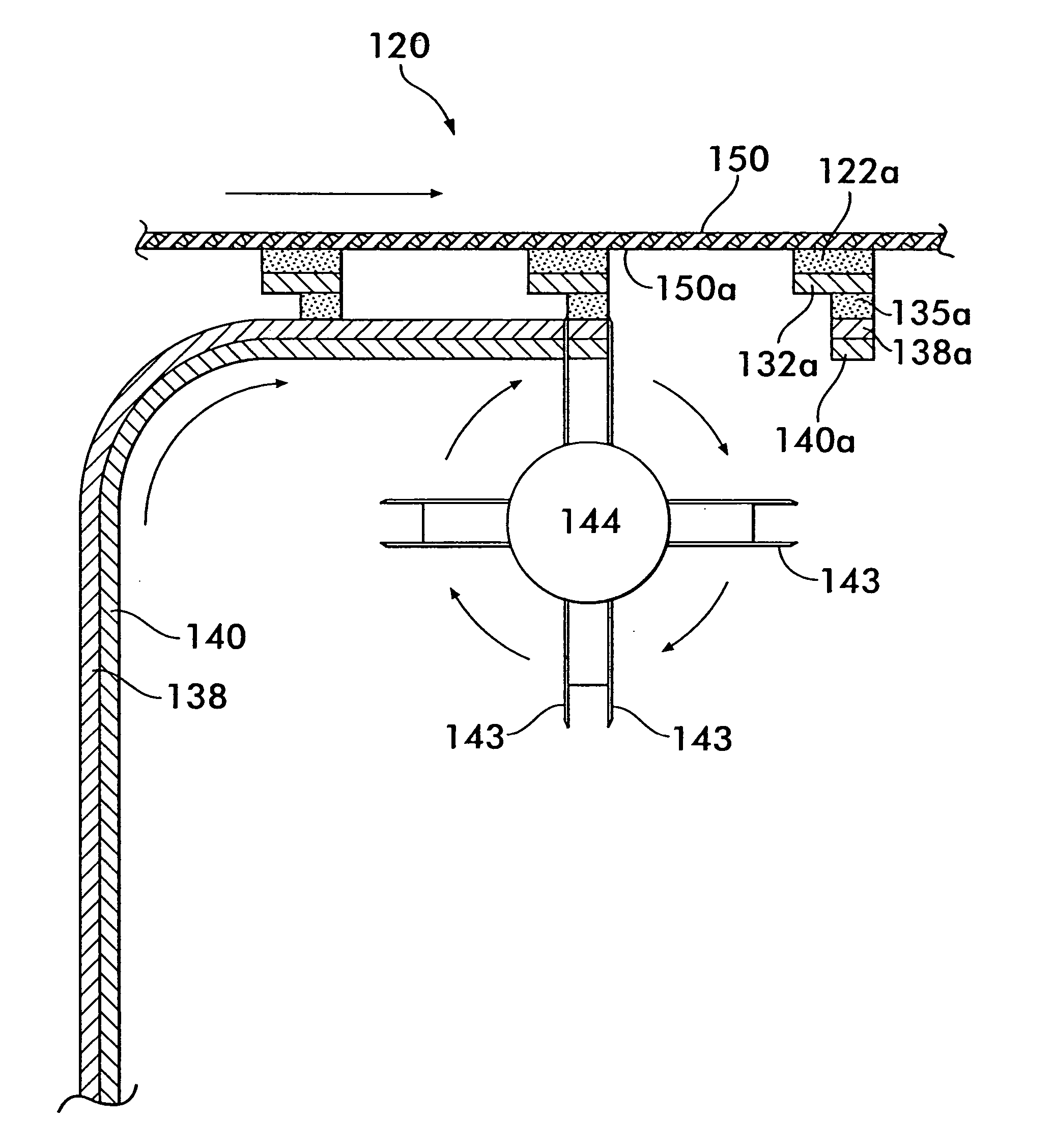
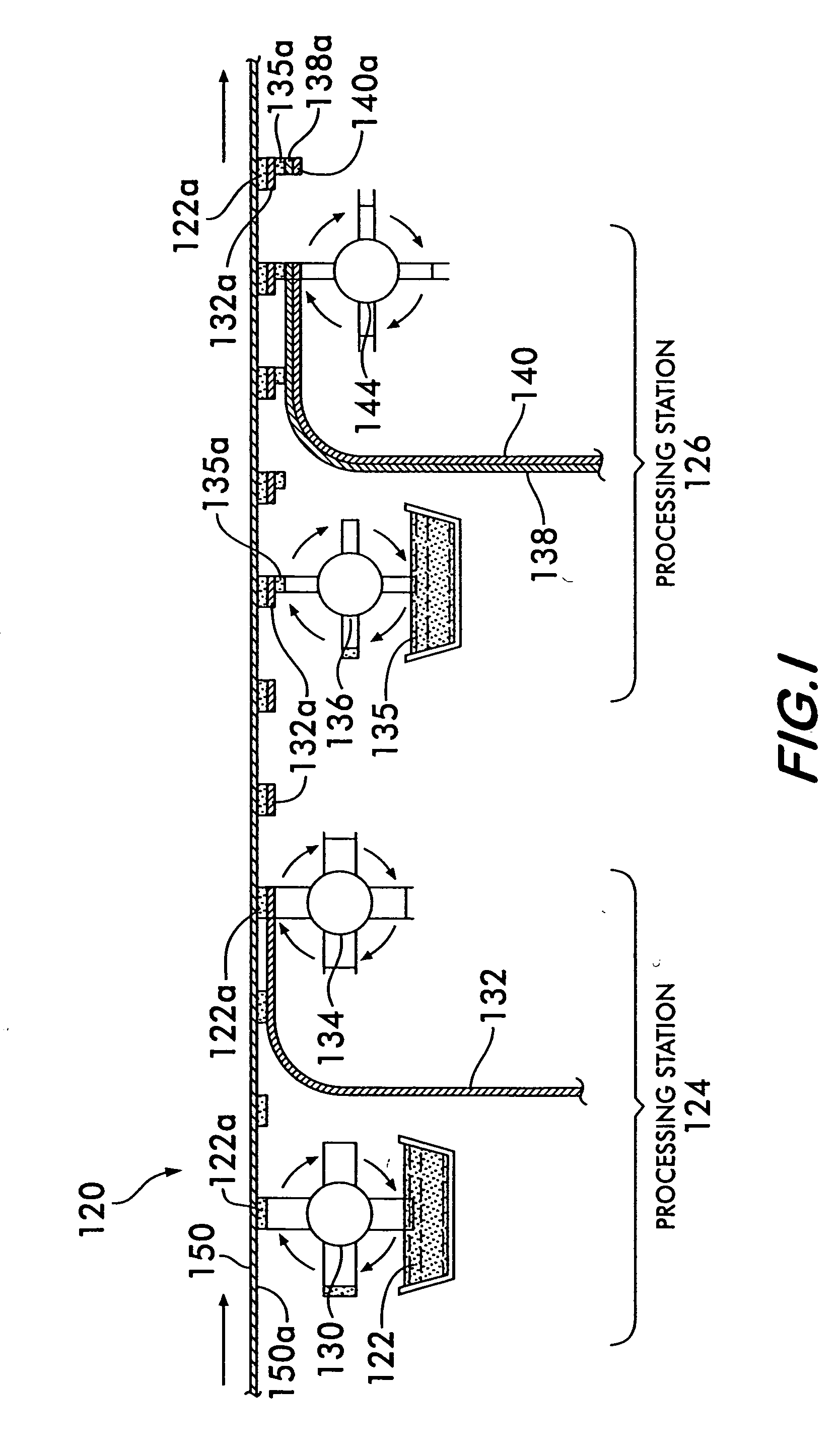
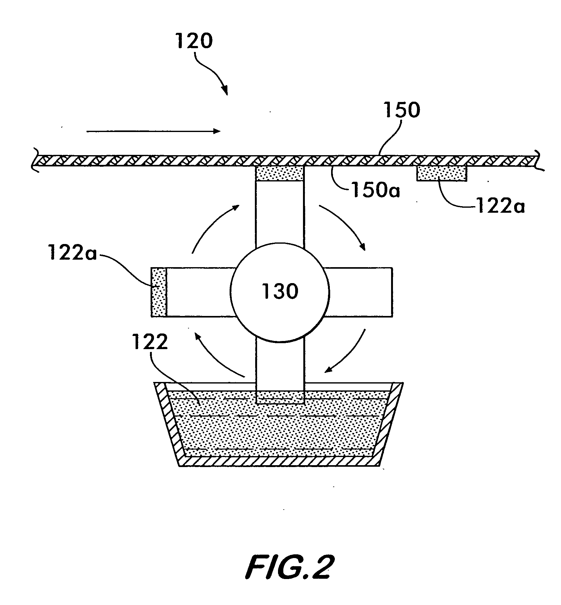
[0064] Referring now to FIG. 1, there is shown a schematic representation of a process 120 for fabricating a security tag according to one preferred embodiment of the invention. The process can be used for producing a security tag having a dipole and a security tag having an inductor and a capacitor. In order to facilitate an understanding of the tag fabrication process 120, FIGS. 2-5 show enlarged representations of selected portions of the schematic representation of FIG. 1.

[0065] In the tag fabrication process 120, an adhesive material 122 is applied to a surface150a of a substrate to form a first patterned adhesive layer 122a. The pattern of the adhesive corresponds to the pattern of the particular portion of the component of the tag, e.g., a portion of the coil of the inductor, a plate of the capacitor, a dipole antenna, etc. The first patterned adhesive layer 122a can be applied to the substrate 150 by an adhesive transfer device 130. The adhesive transfer device 130 can be a...


PUM

PropertyMeasurementUnit
sizeaaaaaaaaaa
sizeaaaaaaaaaa
electromagnetic energyaaaaaaaaaa

Abstract

A circuit element the presence of the circuit element includes first and second capacitor plates disposed over the surface of the substrate in an aligned relationship with each other. The aligned relationship has manufacturing variations in the relative positioning of the first and second capacitor plates and a dielectric layer disposed between the first and second capacitor plates. At least one of the first and second capacitor plates is formed substantially smaller relative to the other of the first and second capacitor plates. The at least one of the capacitor plates is disposed at a predetermined offset in at least one planar direction from an edge of the other of the first and second capacitor plates. The predetermined offset is selected according to the manufacturing variations to prevent variations in the value of capacitance of the capacitor due to the manufacturing variations.

Description

RELATED APPLICATIONS [0001] This is a utility application based upon provisional application Ser. No. 60 / 611,349, filed on Sep. 20, 2004 entitled “Security Tags, Apparatus and Methods for Producing Same”, which was based upon provisional application Ser. No. 60 / 547,235, filed on Feb. 23, 2004 entitled “Security Tags, Apparatus and Methods for Producing the Same.” Applicant hereby claims for this utility application the benefit of the filing date of the provisional application whose entire disclosure are incorporated by reference herein.SPECIFICATION BACKGROUND OF THE INVENTION [0002] 1. Field of Invention [0003] The present invention relates to security tags and, more particularly, to a process for making an electrical circuit for use in a security tag. [0004] 2. Description of Related Art [0005] Security tags are tags that are adapted to reflect electromagnetic energy in order to indicate their presence within a detection zone. They can be associated with an item in order to monito...

Claims


Application Information

Patent Timeline
Patent Type & Authority Applications(United States)
IPC IPC(8): G01V15/00H01G4/005H01G13/00H01Q1/38H01Q9/26H01Q9/28H05K1/16H05K3/04
CPCG01V15/00G06K19/07718G06K19/07786H01G4/005H01G13/00H01Q1/38Y10T29/49117H01Q9/285H05K1/162H05K3/041Y10T29/49133Y10T29/49155H01Q9/265
Inventor ECKSTEIN, ERICCOTE, ANDRE
Owner CHECKPOINT SYST INC
Why Eureka
Try Eureka