Package for electronic component and method of manufacturing piezoelectric device

a piezoelectric device and electronic component technology, applied in the direction of device details, device material selection, piezoelectric/electrostrictive device details, etc., can solve the problems of increased design restrictions and inconvenient manufacturing process management,

Inactive Publication Date: 2005-08-25
SEIKO EPSON CORP
View PDF9 Cites 41 Cited by
  • Summary
  • Abstract
  • Description
  • Claims
  • Application Information

AI Technical Summary

Benefits of technology

[0011] Aspects of the invention address that the positions of the external terminals for connecting to a circuit on a board can easily be changed in accordance with a requirement of a customer. Further, the invention can address that the capacitances of electronic components can easily be varied.
[0013] According to the invention thus arranged, since the connecting electrodes of the component body are connected to different mounting electrodes in the package by changing the equipment (mounting) orientation even with the same component to be accommodated in the package, the positions of the external terminals for operating the component body can be changed. Therefore, by changing the mounting orientation of the component body to the package in accordance with the customer requirements or electronic component models to be manufactured, the external terminals to be connected to the circuit of the board can be selected. Therefore, the freedom of electronic component designing is increased, as well as it becomes possible to easily cope with various requirements of the customers with a common package. Further, since the various specifications are dealt with the same package, stock of the packages or the electronic components can be reduced.
[0015] The invention thus arranged, by rotating the component body to change the mounting orientation, the mounting electrodes to which the connecting electrodes of the component body are bonded can be selected. And, by selecting the mounting electrodes to bonding thereto a pair of connecting electrodes of the component body, a pair of connecting terminals can be electrically connected to a pair of external terminals positioned at the ends of a diagonal or adjacent to each other. Therefore, various specifications required by the customers can easily be dealt with, the number of components need to be stocked can be reduced, thus simplifying the management.
[0017] The invention thus arranged, by rotating the component body to change the mounting orientation, the mounting electrodes to which the connecting electrodes of the component body are bonded can be selected. And, by selecting the mounting electrodes to bonding thereto a pair of connecting electrodes of the component body, a pair of connecting terminals can be electrically connected to a pair of external terminals positioned at the ends of a diagonal or adjacent to each other. Therefore, various specifications required by the customers can easily be dealt with, the number of components need to be stocked can be reduced, thus simplifying the management.
[0019] According to the invention thus arranged, by changing the orientation of the component body when accommodating to the package, the connecting electrodes of the component body can electrically be connected to the different mounting electrodes of the package to change the external terminals for operating the component body. In addition, since the plurality of external terminals is not provided at rotationally symmetric positions, the external terminals in the positions corresponding to the customer requirements can easily be selected. Therefore, the same advantages described above can be provided.
[0025] Further, an exemplary package for an electronic component according to the invention, a package for an electronic component for accommodating the component body, can include a plurality of mounting electrodes, provided to a package body as many as a predetermined number greater than the number of connecting electrodes of the component body, and which is selected in accordance with rotation of the component body to be bonded with connecting electrodes, and a plurality of external terminals formed on a lower surface of the package body, and electrically connected to the mounting electrodes, for bonding with a mounting board. According to the present invention thus arranged, by rotating the component body to select the mounting orientation and then bonding the connecting electrodes provided to the component body with the mounting electrodes, the connecting electrodes can electrically be connected to the different external terminals. Therefore, the positions of the external terminals (mounting terminals) can be changed only by selecting the mounting orientation of the component body in the same package, thus easily dealing with various specifications. Note that a part of the external terminals can be electrically connected to more than one of the mounting electrodes.

Problems solved by technology

However, in recent years, restrictions in designing have been increased as rapid progress of downsizing of electronic devices.
In these cases, capacitors with different capacitances need to be mounted on the boards in related technology, which is inconvenient in view of manufacturing process management.

Method used


Image

  • Package for electronic component and method of manufacturing piezoelectric device
  • Package for electronic component and method of manufacturing piezoelectric device
  • Package for electronic component and method of manufacturing piezoelectric device

Examples


first embodiment

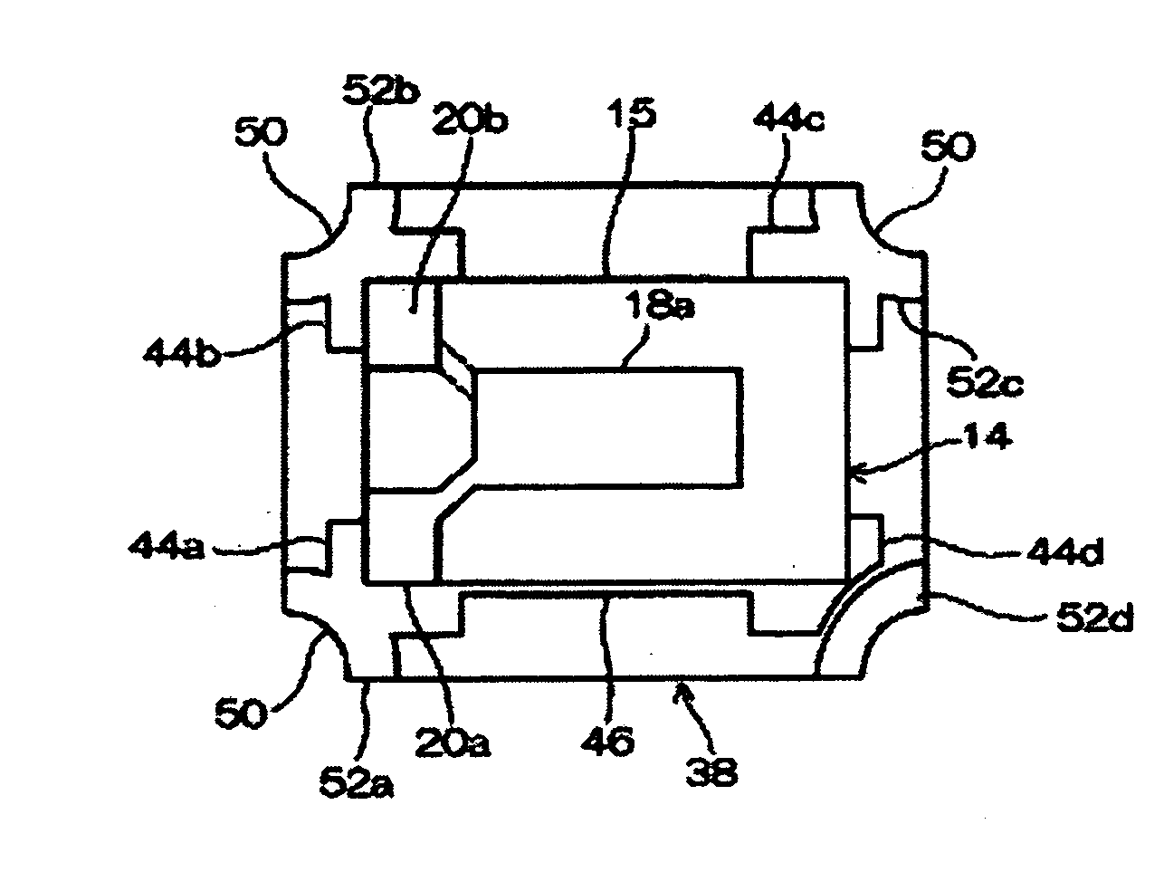
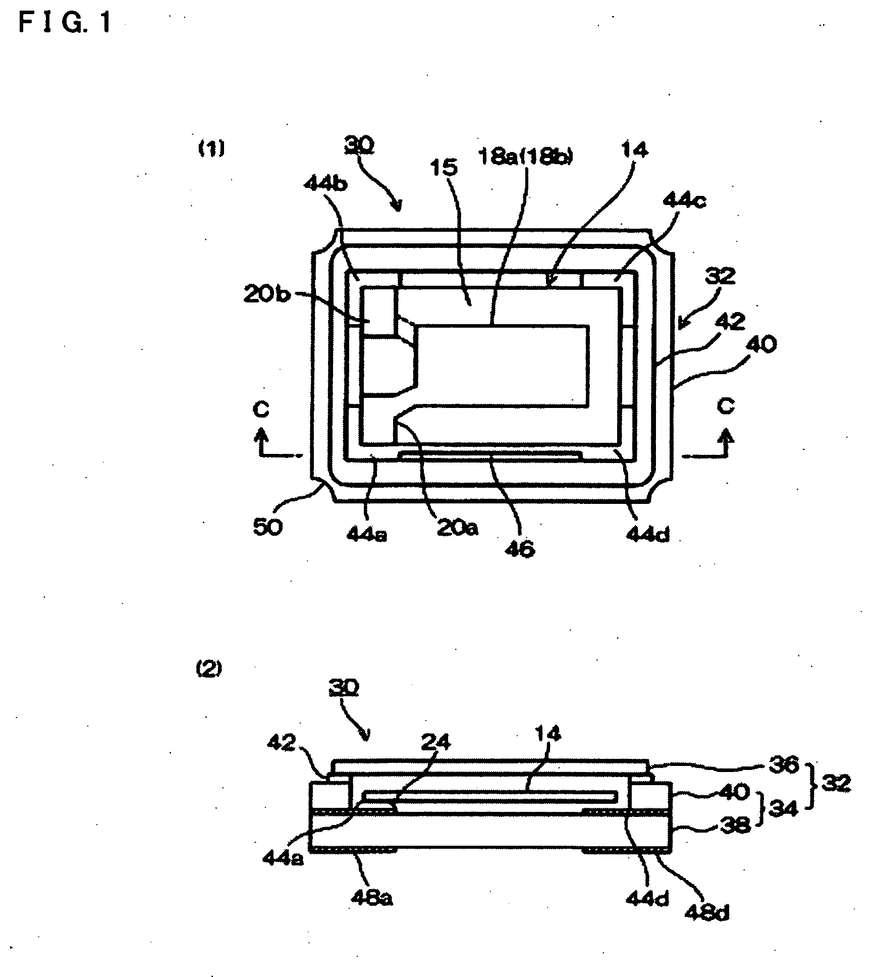
[0048] FIGS. 1(1) and 1(2) explanatorily show an exemplary electronic component using an electronic component package according to the present invention, where FIG. 1(1) is a plan view without the cover and FIG. 1(2) is a cross-sectional view along the C-C line in FIG. 1(1) with the cover.

[0049] In FIGS. 1(1) and 1(2), the piezoelectric resonator 30, which is one of the piezoelectric devices, has the piezoelectric resonator element 14, a component body, contained inside the package 32, as shown in FIG. 1(2). A package 32 can include a package body 34 made of ceramic and a cover 36. The package body 34 is formed of a base sheet 38 shaped like a plate and a frame sheet 40 shaped like a frame stacked and then baked. And, in the embodiment, the cover 36 is made of metal, such as Kovar™, and can be bonded on the upper surface of the frame sheet 40 via seam ring 42 by seam welding to seal the inside of the package 32 airtight.

[0050] On the upper surface of the base sheet 38 defining the ...

second embodiment

[0059] FIGS. 7(1) and 7(2) show a base sheet forming an electronic component package according to the The base sheet 70 is provided with mounting electrodes 72a through 72d for bonding the piezoelectric resonator element 14 not shown in this drawing at the respective corners on the upper surface. As is the case with the first exemplary embodiment, the pair of mounting electrodes 72a, 72b is connected to the conductive patterns 52a, 52b provided around the castellation 50, and is electrically connected to the external terminals 48a, 48b corresponding thereto via the conductive patterns 52a, 52b.

[0060] The other pair of mounting electrodes 72c, 72d is not electrically connected to the external terminals 48c, 48d corresponding thereto because gaps 74, 76 are formed between the pair of mounting electrodes 72c, 72d and the conductive patterns 52c, 52d corresponding thereto. Further, the pair of mounting electrodes 72c, 72d respectively comprises extension patterns 75, 77 extended towar...

third embodiment

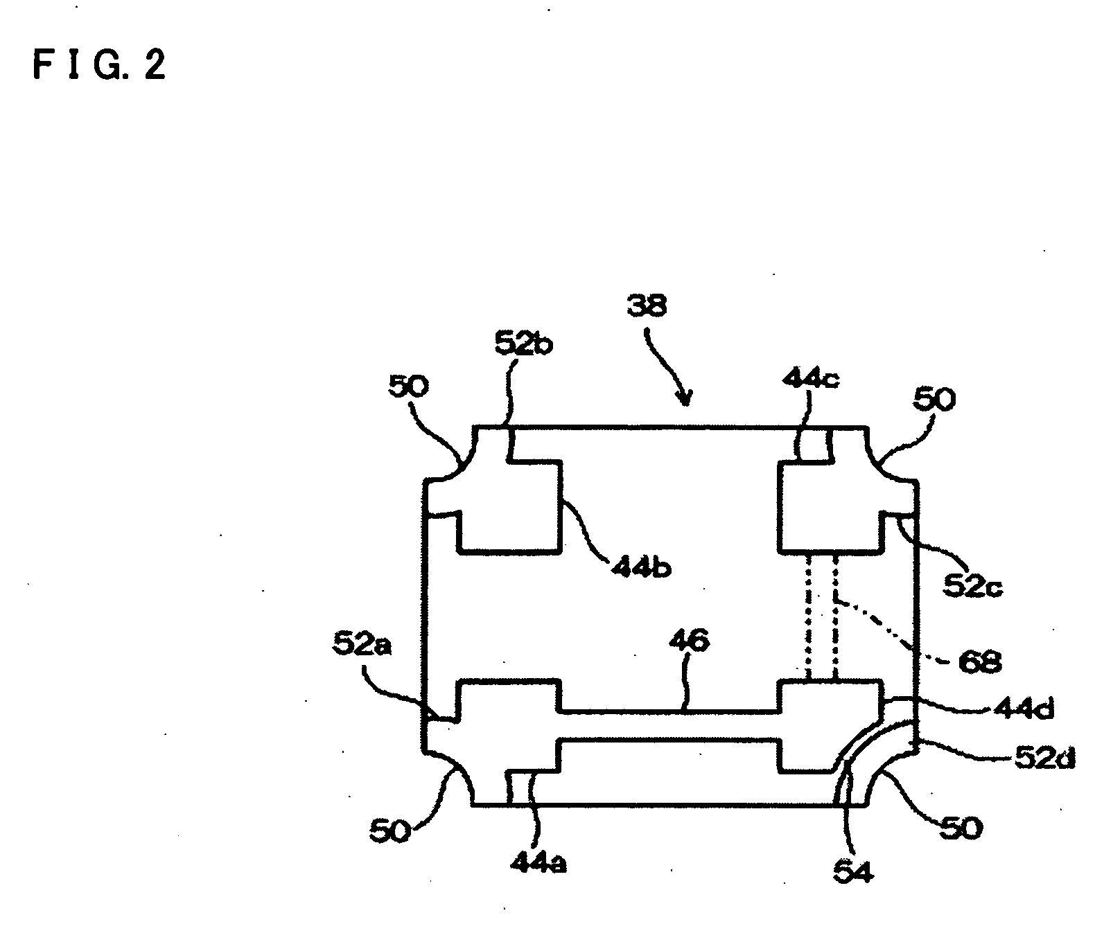
[0062]FIG. 8 shows a pattern of a mounting electrode provided on the upper surface of a base sheet according to the The base sheet 84 is provided with the mounting electrodes 44 (44a through 44d) formed at four corners of the base sheet respectively. Further, a pair of mounting electrodes 44c, 44d of one side respectively has angled extension patterns 86 on the sides in which the mounting electrodes 44b, 44a of the other side are facing thereto. In this regard, the pair of mounting electrodes 44c, 44d has areas larger than the other pair of mounting electrodes 44b, 44a by an area corresponding to the extension pattern 86. And, these mounting electrodes 44 are connected to the conductive patterns 52 corresponding thereto, and are electrically connected via the conductive pattern 52 to the external terminals 48 corresponding thereto not shown in this drawing. Note that each of the external terminals 48a through 48d is electrically isolated from each other.

[0063] Therefore, in case of...


PUM


Abstract

Aspects of the invention provide a package for accommodating a piezoelectric resonator that can include more mounting electrodes than connecting electrodes of the piezoelectric resonator element. The mounting electrodes can be electrically connected with a wiring pattern. In the lower surface of a package body, there can be formed external terminals at the four corners thereof. The external terminals are bonded to a mounting board. The external terminals are electrically connected to the mounting electrodes, respectively. The external terminal is not connected electrically to either of the mounting electrodes. Therefore, positions of the external terminals for operating the piezoelectric resonator can be changed based on whether a pair of connecting electrodes of the piezoelectric vibration element is bonded to the mounting electrodes, or it is connected to the mounting electrodes. Accordingly, it can be possible to easily change positions of external terminals for connecting to a circuit on a board.

Description

BACKGROUND OF INVENTION [0001] 1. Filed of Invention [0002] Aspects of the invention can relate to a package for an electronic component, and especially to a package for an electronic component having a plurality of mounting electrodes for connecting to connection electrodes of the component itself contained in the package and to a method of manufacturing a piezoelectric device. [0003] 2. Description of Related Art [0004] Related art piezoelectric devices, such as quartz resonators or quartz oscillators, as electronic components are contained in surface-mount type packages having main bodies formed with ceramic to have box-shapes in order to meet requirements of smaller-sized or thinner electronic instruments. The piezoelectric devices having such box-shaped packages are often handled with wrong orientations in, for example, right and left direction. And it can be inconvenient that the piezoelectric devices do not normally function when they are mounted with wrong orientations in ri...

Claims


Application Information

Patent Timeline
Patent Type & Authority Applications(United States)
IPC IPC(8): H01L41/04H01L41/08H01L41/18H02N2/00H03B5/32H01L23/04H03H3/02H03H9/02H03H9/05H03H9/10H03H9/15
CPCH03H9/0542H03H9/0547H03H9/0552H03H9/1021H01L2924/3011H01L2224/49171H01L2924/00A63C17/065A63C17/068A63C17/0046A63C17/1436A63C2203/20
Inventor MIYAZAKI, KATSUHIKO
Owner SEIKO EPSON CORP
Why Eureka
Try Eureka