Intelligent full automation controlled flow for a semiconductor furnace tool

a technology of intelligent full automation and furnace tools, applied in the field of intelligent full automation controlled flow of semiconductor furnace tools, can solve the problems of increasing the cost of material handling, underutilizing furnace tools, not being usefully exploited, etc., and achieve the effect of reducing the idle time of processing units

Inactive Publication Date: 2005-08-25
TAIWAN SEMICON MFG CO LTD
View PDF1 Cites 386 Cited by
  • Summary
  • Abstract
  • Description
  • Claims
  • Application Information

AI Technical Summary

Benefits of technology

[0008] In yet another embodiment of the invention a process is adapted to heat and cool a substrate comprising the steps of: forming a first batch of semiconductor material, and loading the first batch into a conveyor, transferring the first batch to a heating mechanism, forming a second batch of semiconductor material, and loading the second batch into a conveyor, while heating the first batch positioned within the heating mechanism; transferring the first batch between a position proximate the heating mechanism and a position proximate the coolable member, cooling the first batch positioned proximate within a cooling mechanism; and while the first batch completes the process, transferring the second batch to a heating mechanism, to reduce the idle time of a processing unit.

Problems solved by technology

Consequently, the furnace tool is underutilized and not usefully exploited because the boat is not loaded with the next batch into the boat before the current batch completes its inspection.
The process quality check decreases the efficiency of furnace tool use and increases the cost of material handling, generally.

Method used


Image

  • Intelligent full automation controlled flow for a semiconductor furnace tool
  • Intelligent full automation controlled flow for a semiconductor furnace tool
  • Intelligent full automation controlled flow for a semiconductor furnace tool

Examples


Embodiment Construction

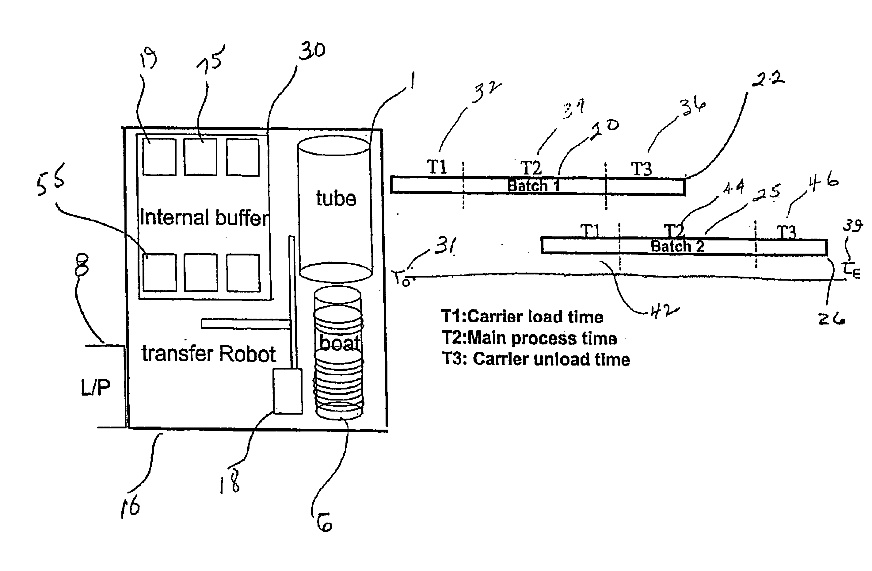
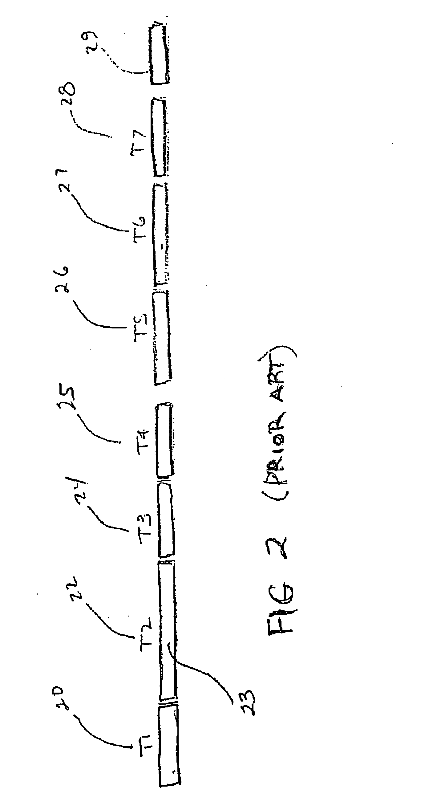
[0015] As previously indicated the furnace may be divided into two major parts: one a transfer unit and the other a tube unit. The transfer unit transfers wafers from the FOUP into the tube unit, removes wafer batches from the tube unit and moves the FOUP into and out of the tool. When tube unit is processing wafers, the transfer unit is typically in an idle state. When transfer unit is active, the tube is in an idle state. In most implementations of furnace, two or more batches may be stored on an internal buffer in the FOUP to reduce the idle time of transfer.

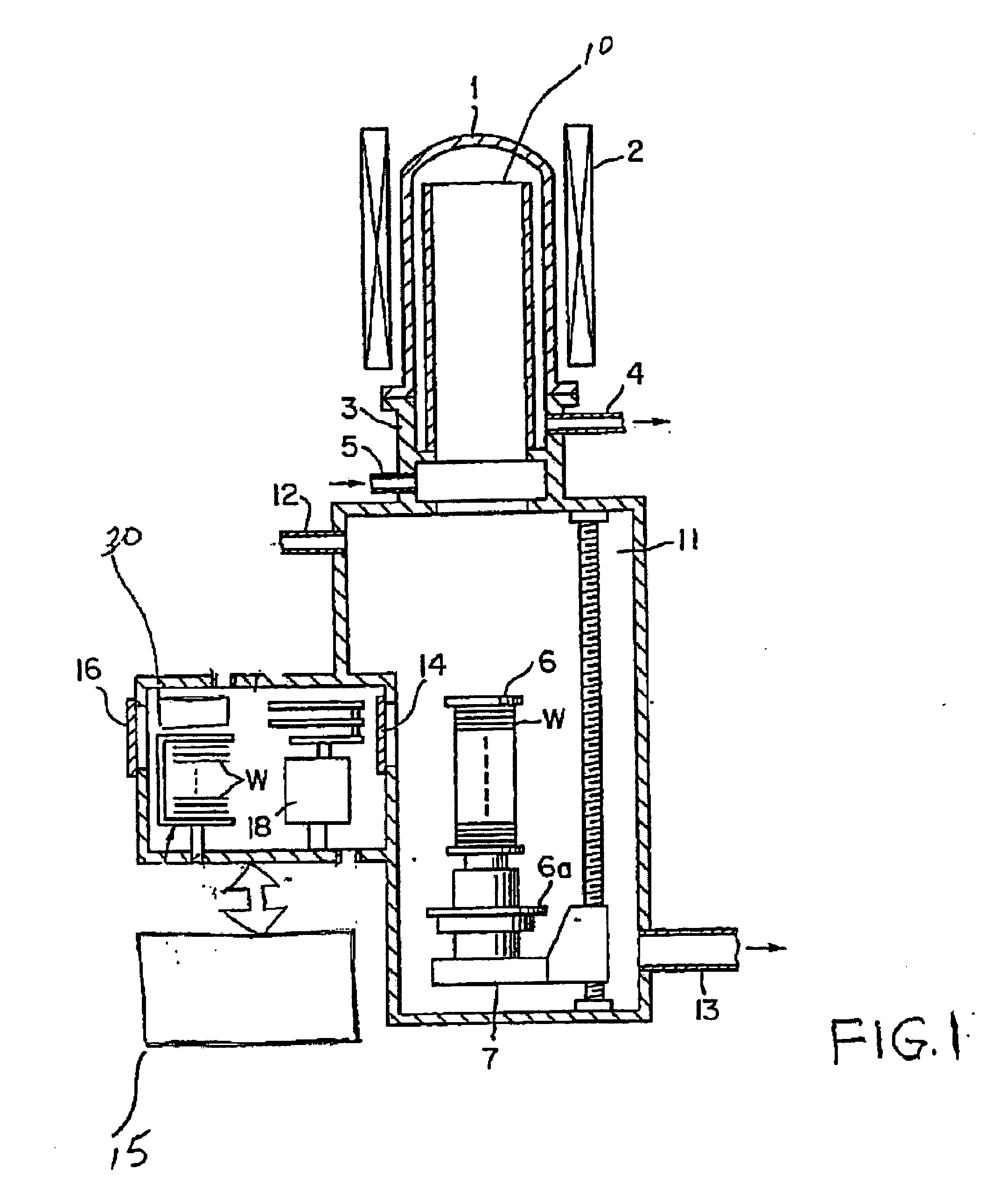
[0016] Referring to FIG. 1, in a front-opening unified pod furnace tool 1, semiconductor wafers W are transported by a transfer robot 18 that serves as a conveying mechanism, that carries one batch of wafers W via a transfer robot 18 into a vacuum chamber 11 to a wafer boat 6 in the chamber 11 through the gate 14. It is understood that the next batch of wafers W to be processed must await the current batch's process completi...


PUM


Abstract

The present invention relates to an apparatus and method for processing the flow of semiconductor wafers through a furnace tool having a front-opening unified pod (FOUP) material handling system. The invention provides for an automated control flow to realize greater efficiency and assure process quality. In one aspect of the invention the wafer batch completing its operation is discharged simultaneous with the charging of the next batch. Essentially the operation takes place by overlapping processing operations. An embodiment of the invention includes a process comprising the steps of: providing a first batch of semiconductor material, and loading the first batch into a carrier which transports the first batch into a semiconductor manufacturing process, and while the first batch undergoes the process, forming a second batch of semiconductor material, and pausing a second batch process operation until the first batch completes processing, to reduce the idle time of said process.

Description

BACKGROUND OF THE INVENTION [0001] 1. Field of the Invention [0002] The present invention relates to methods for processing the flow of semiconductor wafers through a furnace tool having a front-opening unified pod material handling system (“FOUP”). [0003] 2. Description of the Prior Art [0004] The present invention is drawn to a furnace utilized in the fabrication of semiconductor devices where materials in the form of wafers are batched and automatically conveyed into a processing chamber. As shown in FIG. 1, semiconductor wafers are transported by a transfer robot that serves as a conveying mechanism, that carries one batch of wafers via a transfer robot into a vacuum chamber to a wafer boat in the processing chamber through the gate that separates the chamber from the storage area. Wafers awaiting processing must sit idle until the current batch's process cycle is complete. Wafers are placed into the wafer boat and lifted by a boat elevator into a processing tube. The processing...

Claims


Application Information

Patent Timeline
Patent Type & Authority Applications(United States)
IPC IPC(8): G06F19/00H01L21/00H01L21/677
CPCH01L21/67757H01L21/67276
Inventor WANG, KUO-HUACHEN, SHUN-AN
Owner TAIWAN SEMICON MFG CO LTD
Why Eureka
Try Eureka