Slew rate controlled output driver for use in semiconductor device

a technology of output driver and semiconductor device, which is applied in the direction of pulse manipulation, pulse technique, instruments, etc., can solve the problems of switching noise reduction, voltage level change in shorter time, and importance of slave rate control

Inactive Publication Date: 2005-09-08
SK HYNIX INC
View PDF13 Cites 30 Cited by
  • Summary
  • Abstract
  • Description
  • Claims
  • Application Information

AI Technical Summary

Benefits of technology

[0022] It is, therefore, an object of the present invention to provide an output driver for use in a semiconductor, for capable of maintaining its slew rate constantly regardless of PVT(Process / Voltage / Temperature) variation.

Problems solved by technology

With regard to the push-pull type driver, slew rate control becomes an importance issue.
In any case, the larger slew rate shows the more abrupt slope of the output signal, which means the voltage level changes in shorter time.
To the contrary, when the slew rate is small, the switching noise decreases but the data skew increases, even to the extent that the signal shows the transition before the level of the output signal reaches its peak point.
However, with this scheme, a problem occurs when there is any PVT(Process / Voltage / Temperature) variation.
Though such a problem was not so serious with low transmission rate, it would burden significantly in accomplishing higher transmission rate such as over 800 Mbps and even over 1 Gbps.
In this case, the switching noise decreases greatly because current value of the output signal varies slowly.
However, there is a problem such that the slew rate is not robust for PVT variation because the delay amounts of the delay elements in the first and second delays 30, 32 vary depending on PVT variation.
Further, in this approach, there is a high transmission problem because of inevitable output delay.
However, because that this waveform contains much noise, ISI and so on, it not easy to adjust the output waveform with feedback.

Method used


Image

  • Slew rate controlled output driver for use in semiconductor device
  • Slew rate controlled output driver for use in semiconductor device
  • Slew rate controlled output driver for use in semiconductor device

Examples


Embodiment Construction

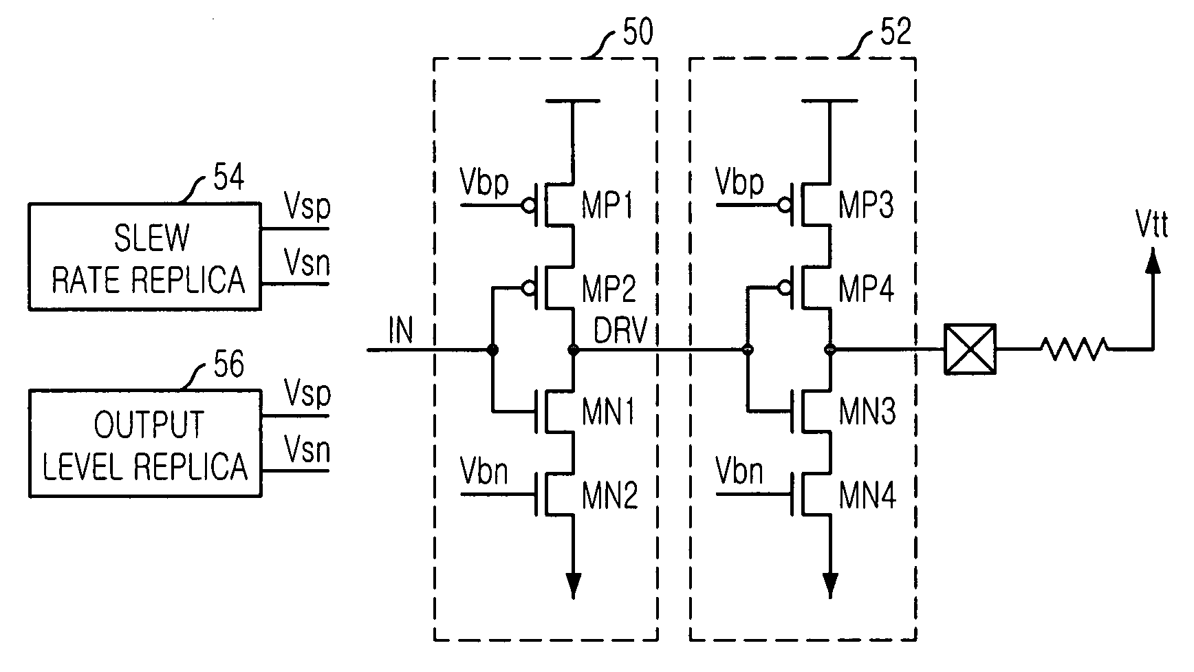
[0041] Hereinafter, an output driver for use in a semiconductor device in accordance with the present invention will be described in detail referring to the accompanying drawings.

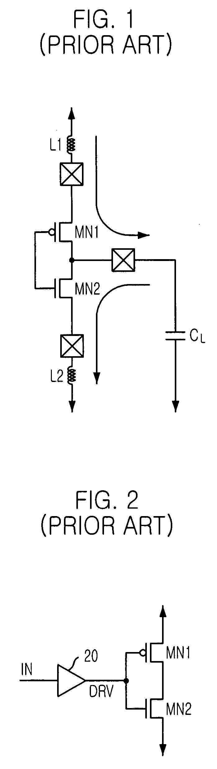
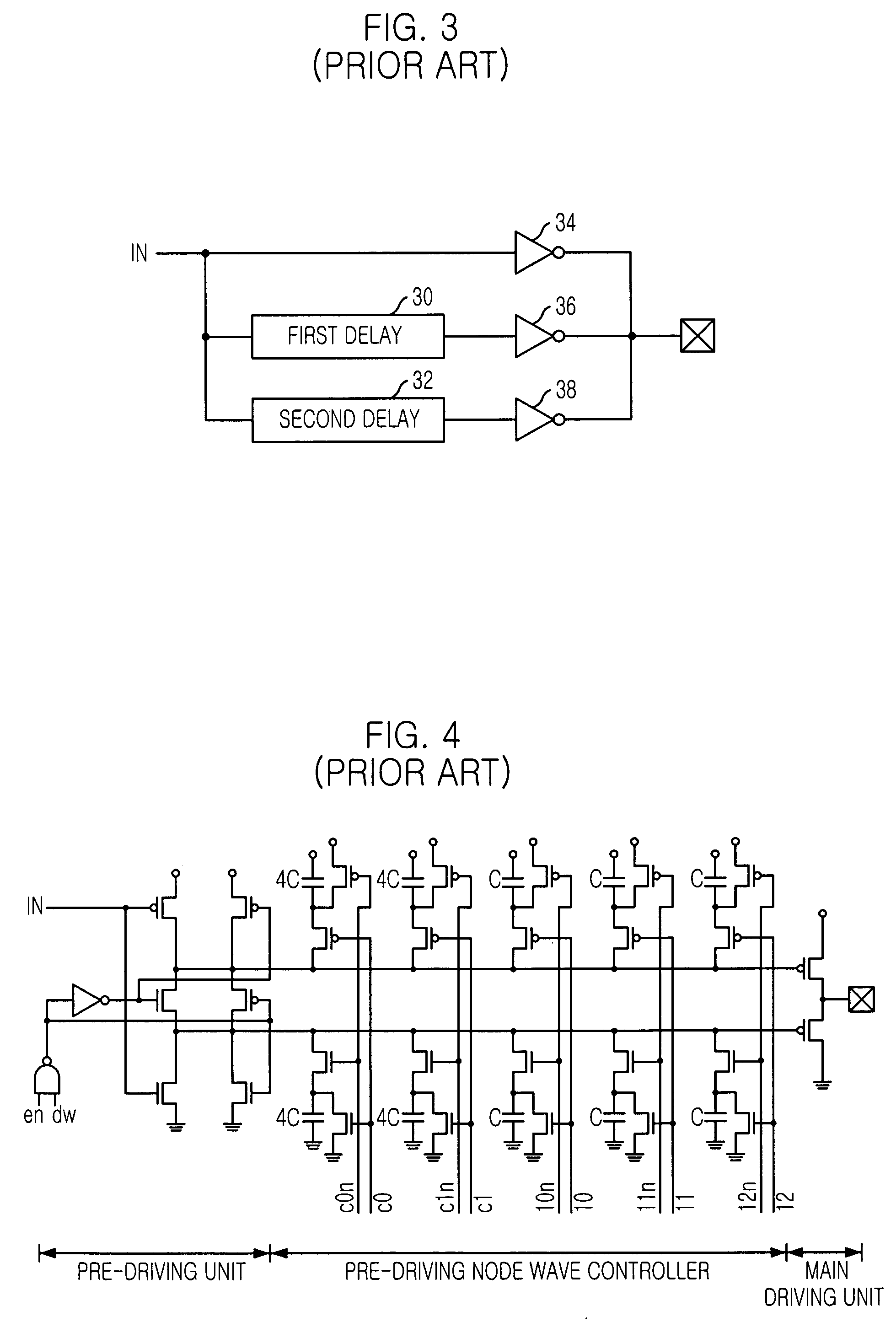
[0042] The present invention employs an output driver of SSTL type push-pull structure because it is difficult to control slew rate because a waveform in pull-up operation is determined only with passive elements while the waveform in pull-down operation can be controlled somehow with open drain technique. Therefore, a push-pull type output driver is targeted to adjust by itself for both pull-up and pull-down operations. On the other hand, instead of the conventional binary weighting technique, the slew rate is adjusted by using only one transistor with replica bias technique in the present invention.

[0043] Hereinafter, it will be described for a preferred embodiment of the present invention for those skilled in the art to readily practice the present invention.

[0044]FIG. 5 is a circuit diagram showing a...


PUM


Abstract

An output driver for use in a semiconductor is capable of maintaining its slew rate constantly regardless of PVT(Process / Voltage / Temperature) variation. The output driver includes a pre-driving unit for pre-driving a data signal; a main driving unit for driving an output pad in response to the output signal of the pre-driving unit; and a slew rate modeling unit for generating a pre-driver bias signal to constantly maintain effective resistances of a pull-up path and a pull-down path of the pre-driving unit by modeling the pre-driving unit.

Description

FIELD OF INVENTION [0001] The present invention relates to a semiconductor circuit technique; and, more particularly, to an output driver for use in a semiconductor device. DESCRIPTION OF PRIOR ART [0002] An output driver for use in a semiconductor device is a driving circuit for driving an output pad coupled to a certain load to output data from an internal element to any external element. [0003] Generally, a push-pull type driver has been widely used as such an output driver. With regard to the push-pull type driver, slew rate control becomes an importance issue. [0004] The slew rate is an index for representing how fast the voltage level of the output signal changes, which may be defined as a slope depicting voltage level change per unit time. On the other hand, there are up slew rate and down slew rate in the slew rate. The up slew rate represents the slope when the voltage level of the output signal has a transition from a low level to a high level while the down slew rate repr...

Claims


Application Information

Patent Timeline
Patent Type & Authority Applications(United States)
IPC IPC(8): G11C7/10H03B1/00
CPCG11C7/02G11C7/04G11C7/1057H03K19/018521H03K17/164H03K19/01721G11C7/1084A63C17/0046A63C17/223A63C2203/20
Inventor CHOI, SEOK-WOOPARK, HONG-JUNE
Owner SK HYNIX INC
Why Eureka
Try Eureka