Method of and inductor layout for reduced VCO coupling

a technology of inductance layout and coupling, which is applied in the direction of transformer/inductance coil/winding/connection, waveguide type devices, inductance, etc., can solve the problems of increasing current consumption, spurious receiver responses and unwanted frequencies in the transmit spectrum, and integrating a complete rf transceiver on a single chip. , to achieve the effect of reducing electromagnetic field, reducing mutual electromagnetic coupling, and reducing electromagnetic field

Active Publication Date: 2005-09-08
TELEFON AB LM ERICSSON (PUBL)
View PDF12 Cites 104 Cited by
  • Summary
  • Abstract
  • Description
  • Claims
  • Application Information

AI Technical Summary

Benefits of technology

[0008] In general, in another aspect, an inductor layout having reduced mutual electromagnetic coupling comprises a first inductor having a shape that is substantially symmetrical about a first predefined axis, the shape causing the first inductor to have a reduced electromagnetic field at a certain distance from the first inductor, at least in some directions. The inductor layout further comprises a second inductor positioned at a predetermined distance from the first inductor, wherein a mutual electromagnetic coupling between the first inductor and the second inductor is reduced as a result of the first inductor having a reduced electromagnetic field.

Problems solved by technology

However, integrating a complete RF transceiver on a single chip presents a number of challenges.
Such an arrangement may produce undesired interaction between the two VCOs due to various types of mutual coupling mechanisms, which may result in spurious receiver responses and unwanted frequencies in the transmit spectrum.
However, these solutions require additional circuitry (dividers, mixers, etc.) that may increase current consumption, making them less attractive than other mutual EM coupling reduction alternatives.

Method used


Image

  • Method of and inductor layout for reduced VCO coupling
  • Method of and inductor layout for reduced VCO coupling
  • Method of and inductor layout for reduced VCO coupling

Examples


Embodiment Construction

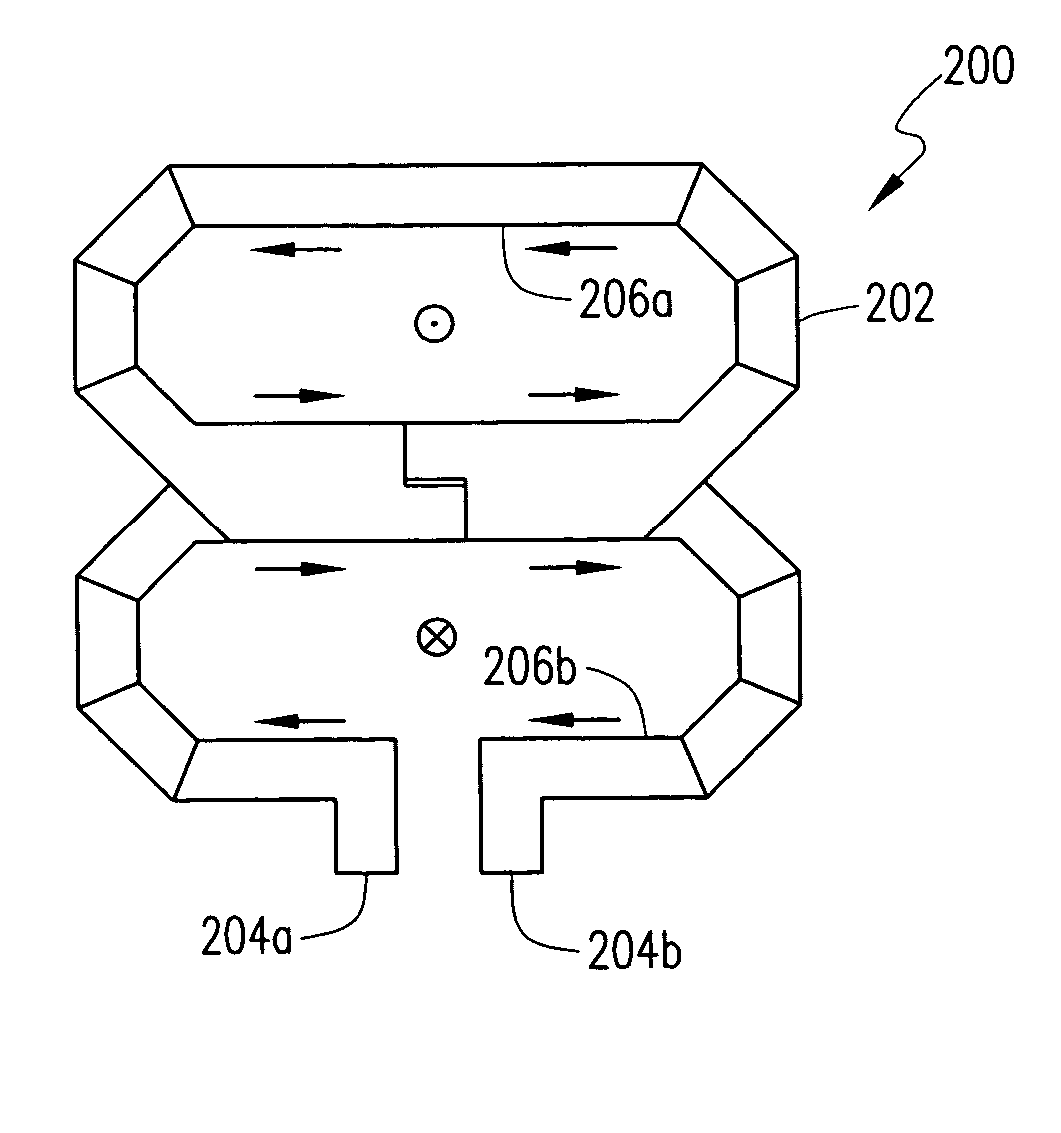
[0024] As mentioned above, various embodiments of the invention provide an inductor design and method of implementing the same where mutual EM coupling is reduced. The inductor design and method serve to reduce the EM field at a certain distance from the inductor (i.e., the far field), at least in some directions, by using inductor shapes that are substantially symmetrical. As used herein, the term “symmetrical” refers to symmetry relative to at least one axis. This reduced far field may then be used to reduce the mutual coupling between two inductors. The inductor design and method may also be used to reduce the coupling between an inductor and another on-chip or external structure (e.g., an external power amplifier). This helps reduces the sensitivity of the VCO to interfering signals from other than a second on-chip VCO.

[0025] Choosing a substantially symmetrical shape (e.g., a figure-8 or a four-leaf clover shape) for the first inductor helps reduce the EM field at far distance...


PUM

PropertyMeasurementUnit
sizeaaaaaaaaaa
center distanceaaaaaaaaaa
distanceaaaaaaaaaa

Abstract

Method and system are disclosed for reducing mutual EM coupling between VCO resonators and for implementing the same on a single semiconductor chip. The method and system involve using inductors that are substantially symmetrical about their horizontal and/or their vertical axes and providing current to the inductors in a way so that the resulting magnetic field components tend to cancel each other by virtue of the symmetry. In addition, two such inductors may be placed near each other and oriented in a way so that the induced current in the second inductor due to the magnetic field originating from first inductor is significantly reduced. The inductors may be 8-shaped, four-leaf clover-shaped, single-turn, multi-turn, rotated relative to one another, and/or vertically offset relative to one another. This Abstract is submitted with the understanding that it will not be used to interpret or limit the scope or meaning of the claims.

Description

CROSS-REFERENCE TO RELATED APPLICATIONS [0001] This application claims priority from, and hereby incorporates by reference the entire disclosure of, U.S. Provisional Application No. 60 / 549,611, bearing Docket No. 53807-00113USPL, entitled “Inductor Design for Reduced VCO Coupling”, and filed on Mar. 3, 2004.FIELD OF THE INVENTION [0002] The present invention relates to voltage-controlled oscillators (VCO) of the type used in radio frequency (RF) transceivers and, in particular, to an improved inductor design in a VCO. BACKGROUND OF THE INVENTION [0003] Recent advances in wireless communication technology have allowed an entire RF transceiver to be implemented on a single semiconductor die or chip. However, integrating a complete RF transceiver on a single chip presents a number of challenges. For example, in wideband code division multiple access (WCDMA) transceivers, a single-chip solution requires two RF VCOs to be running on the chip at the same time. Such an arrangement may prod...

Claims


Application Information

Patent Timeline
Patent Type & Authority Applications(United States)
IPC IPC(8): H01F17/00H01F27/34H01L27/08
CPCH01F27/346H01F17/0006H01F2017/0073H01F17/00
Inventor MATTSSON, THOMAS
Owner TELEFON AB LM ERICSSON (PUBL)
Why Eureka
Try Eureka