Chemical mechanical polishing method, chemical mechanical polishing system, and manufacturing method of semiconductor device

Inactive Publication Date: 2005-09-08
TRECENTI TECHNOLOGIES INC
View PDF5 Cites 18 Cited by
  • Summary
  • Abstract
  • Description
  • Claims
  • Application Information

AI Technical Summary

Benefits of technology

[0024] An object of the present invention is to set a polishing rate and a polishing time in the chemical mechanical polishing with high accuracy.
[0030] Also, by use of a conversion table from which a polishing rate set from a layer-forming material and a polishing condition can be easily read, setting of the polishing time of one layer of a multi-layer structure can be easily carried out by converting the polishing time of one layer to that of a particular layer thereof.
[0033] By correcting the polishing rate on the basis of the past polishing records of actual product wafers, calculation accuracy of the polishing rate can be further enhanced. Therefore, a polishing process can be made more efficient.

Problems solved by technology

However, the present inventors have found out that the above-described technique for setting the polishing rate has the following problems.
That is, since the polishing rate is different depending on the pattern shape of the object to be polished, or the quality of the film to be polished, the technique disclosed in Patent Document 1 is a technique for setting the polishing pattern unsuitable for producing various types of products.
Also, in the technique, any method of determining the calculating formula for calculating the optimum polishing time is not described, so that the way how the polishing rate should be calculated is unclear.
However, definition of such weighting is unclear.
Therefore, definition of the estimation polishing rates per se is ambiguous and accuracy of the estimation polishing rates to be calculated cannot be assured.
Furthermore, if the model calculating formula is deviated from the actual one, there is the drawback of being unable to control the polishing amount or polishing time since a function of correcting the deviation is not provided.

Method used


Image

  • Chemical mechanical polishing method, chemical mechanical polishing system, and manufacturing method of semiconductor device
  • Chemical mechanical polishing method, chemical mechanical polishing system, and manufacturing method of semiconductor device
  • Chemical mechanical polishing method, chemical mechanical polishing system, and manufacturing method of semiconductor device

Examples


first embodiment

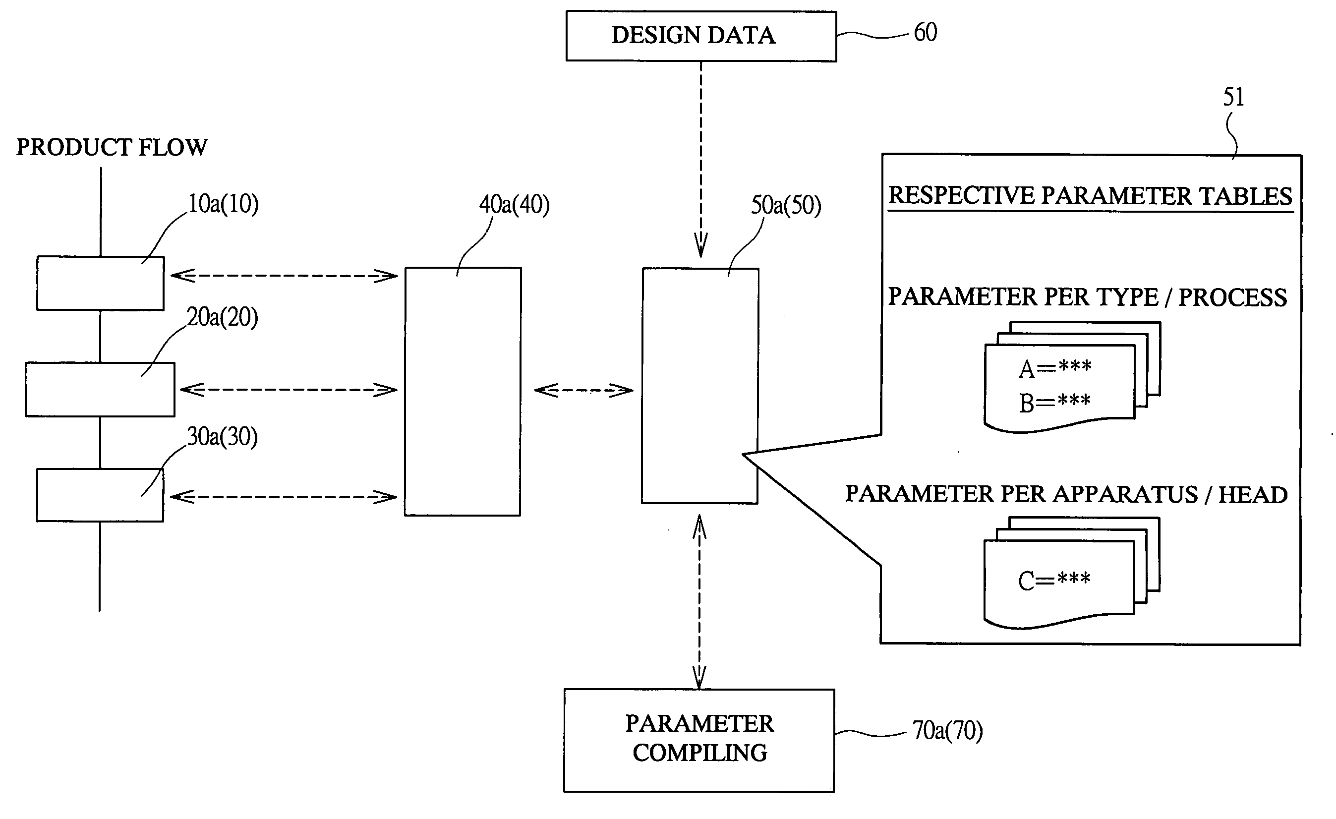
[0045] In a chemical mechanical polishing method of the present invention, a polishing condition such as a polishing rate or polishing time is calculated by use of a novel calculating formula, whereby chemical mechanical polishing is carried out. The novel calculating formula comprises a term dependent on a product wafer that is an object to be subjected to the chemical mechanical polishing and a term dependent on an apparatus for performing the chemical mechanical polishing to the product wafer, wherein the respective terms are combined by operators.

[0046] Under the condition that it is assumed that influences of the chemical mechanical polishing apparatus to be used on polishing conditions are the same, the term dependent on the product wafer has at least a parameter “A” exclusively representing influences of a film property such as film quality on the polishing condition, and a parameter “B” exclusively representing influences of a roughness state such as concave / convex patterns...

second embodiment

[0158] In a chemical mechanical polishing method for a multi-layer structure comprising a plurality of stacked films, which is the present invention, when a polishing rate of a certain stacked film among the plurality of stacked films that are objects to be subjected to the chemical mechanical polishing is converted is converted into that of another stacked film and when each polishing time of the chemical mechanical polishing of the plurality of stacked films that are objects to be polished is to be set, this embodiment employs a novel conversion table by which the conversion results can be distinctly easily determined.

[0159] In the chemical mechanical polishing of the multi-layer structure, the above-described novel calculating formulas found out by the present inventors can be employed, and a polishing condition such as a polishing rate or polishing time is calculated, thereby allowing the chemical mechanical polishing to be performed with higher accuracy.

[0160] In the present ...

third embodiment

[0181] In the above second embodiment, there has been described the case where the multi-layer structure “S” shown in FIG. 5A comprises the first-layer (uppermost-layer) stacked film 300 and the second-layer stacked film 200 corresponding to a non-uppermost layer and the polishing times are calculated by converting the polishing rate of the second-layer stacked film 200 to that of the stacked film 300. However, it has newly become clear that use of the conversion table shown in FIG. 6 can be applied to a chemical mechanical polishing method other than the above-described chemical mechanical polishing method.

[0182] That is, the description of the second embodiment is about the case where one of the stacked films of different types is converted to the other to carry out the chemical mechanical polishing under the same polishing condition. However, it can be seen in the conversion table that the selection ratio of a combination of the film type “A” and the polishing condition α is the...


PUM

PropertyMeasurementUnit
Timeaaaaaaaaaa
Surface roughnessaaaaaaaaaa

Abstract

Setting a polishing rate and a polishing time in chemical mechanical polishing can be performed with high accuracy by considering a product wafer of an object to be polished, and an instrumental error between apparatuses to be used, etc. By using, as a calculating formula, a formula well approximating a portion of a curve representing a state of chemical mechanical polishing on a side showing a target polishing amount, the polishing rate and the polishing time can be set with high accuracy according to a state of chemical mechanical polishing for actually polishing a product wafer. In the calculating formula, a parameter “A” relating to a film property of a film of an object to be polished, a parameter “B” relating to a roughness state of a film surface, and a parameter “C” relating to an instrumental error differential between apparatuses of a chemical mechanical polishing apparatus are joined by operators.

Description

CROSS-REFERENCE TO RELATED APPLICATION [0001] The present application claims priority from Japanese patent application No. JP 2004-061284 filed on Mar. 4, 2004 and No. 2004-378751 filed on Dec. 28, 2004, the contents of which are hereby incorporated by reference into this application. BACKGROUND OF THE INVENTION [0002] The present invention relates to manufacturing techniques of semiconductor devices, and particularly relates to techniques effectively applied to calculating, with high accuracy, a polishing condition such as a polishing rate in chemical mechanical polishing (CMP) based on past polishing records. Also, the polishing condition such as a polishing rate can be utilized for making the calculation easy and high accuracy in performing the chemical mechanical polishing to stacked films. [0003] The below described techniques have been studied by the present inventors for accomplishing the present invention, and the outline thereof is as follows. [0004] Recently, as demands fo...

Claims


Application Information

Patent Timeline
IPC IPC(8): B24B1/00B24B37/00B24B49/00H01L21/304
CPCB24B49/03B24B37/005A61H39/086C23C14/165C23C14/3414C23C14/0036
Inventor AOYAGI, MASAHIRONAKAJO, AKITSUCHIYAMA, HIROFUMINAKAMURA, SHINOBU
Owner TRECENTI TECHNOLOGIES INC
Why Eureka
Try Eureka