Orientated group IV-VI semiconductor structure, and method for making and using the same

a technology of semiconductor structure and orientated group, which is applied in the direction of lasers, bulk negative resistance effect devices, semiconductor lasers, etc., can solve the problems of limited tuning range and performance of vcsels, and the performance of these vcsels remains far from the desired level, so as to achieve the effect of improving performan

Inactive Publication Date: 2005-09-15
THE BOARD OF RGT UNIV OF OKLAHOMA
View PDF6 Cites 25 Cited by
  • Summary
  • Abstract
  • Description
  • Claims
  • Application Information

AI Technical Summary

Benefits of technology

[0013] The present invention explores, for the first time, fabrication of devices using IV-VI lead salt materials on a [110] substrate. Theoretical and preliminary experimental results for the present invention show that [110] orientated IV-VI quantum well (QW) structures have much higher material gain than other orientations, such as [100] and [111] orientations, as discussed further in “[110] Orientated Lead Salt Mid-Infrared Lasers,”Applied Physics Letters, 85, 2999 (2004), the entire content of which is hereby expressly incorporated herein by reference. In addition, the expected material quality of expitaxial layers on the [110] orientation is higher due to the easy dislocation gliding. Therefore, all devices using IV-VI materials orientated along the [110] direction will benefit. For example, fabrication of laser structures using [110] orientated IV-VI materials are given as examples of such devices herein. However, other devices such as detectors, thermal electrical cooling devices, solar cells, etc., can all be fabricated on a [110] orientation and therefore have improved performances.
[0015] The [110] orientated IV-VI semiconductor structure of the present invention provides high material quality, high modal gain, suppressed Auger non-radiative loss, light electron and hole masses, and lifts in degeneracy to reduce lasing threshold. A laser device utilizing the IV-VI semiconductor structure having a [110] orientation, which is constructed in accordance with the present invention, also has reproducibility over a broad range of wavelengths and can operate at continuous mode. Further, in one embodiment, a laser device can be provided with a ridge wave-guide structure with a thick gold plating to improve heat dissipation, thus obtaining a high continuous wave (CW) operating temperature, and single mode operation with a small ridge width.

Problems solved by technology

However, their performance remains far from that desired because of their low operating temperatures and low efficiencies (single-mode output powers are typically≦1 mW, even at 77 K).
However, while these previous VCSELs on [111] orientated BaF2 substrates have proven successful in some aspects, the tuning and tuning range (as determined by cavity mode tuning) of these VCSELs have been limited.
While problems of material quality, efficiency, gain, etc., associated with various semiconductor structures have been generally described above with reference to laser devices, these same problems are also seen in semiconductor structures used in other electronic applications, including optoelectronic and thermoelectronic applications.

Method used


Image

  • Orientated group IV-VI semiconductor structure, and method for making and using the same
  • Orientated group IV-VI semiconductor structure, and method for making and using the same
  • Orientated group IV-VI semiconductor structure, and method for making and using the same

Examples


Embodiment Construction

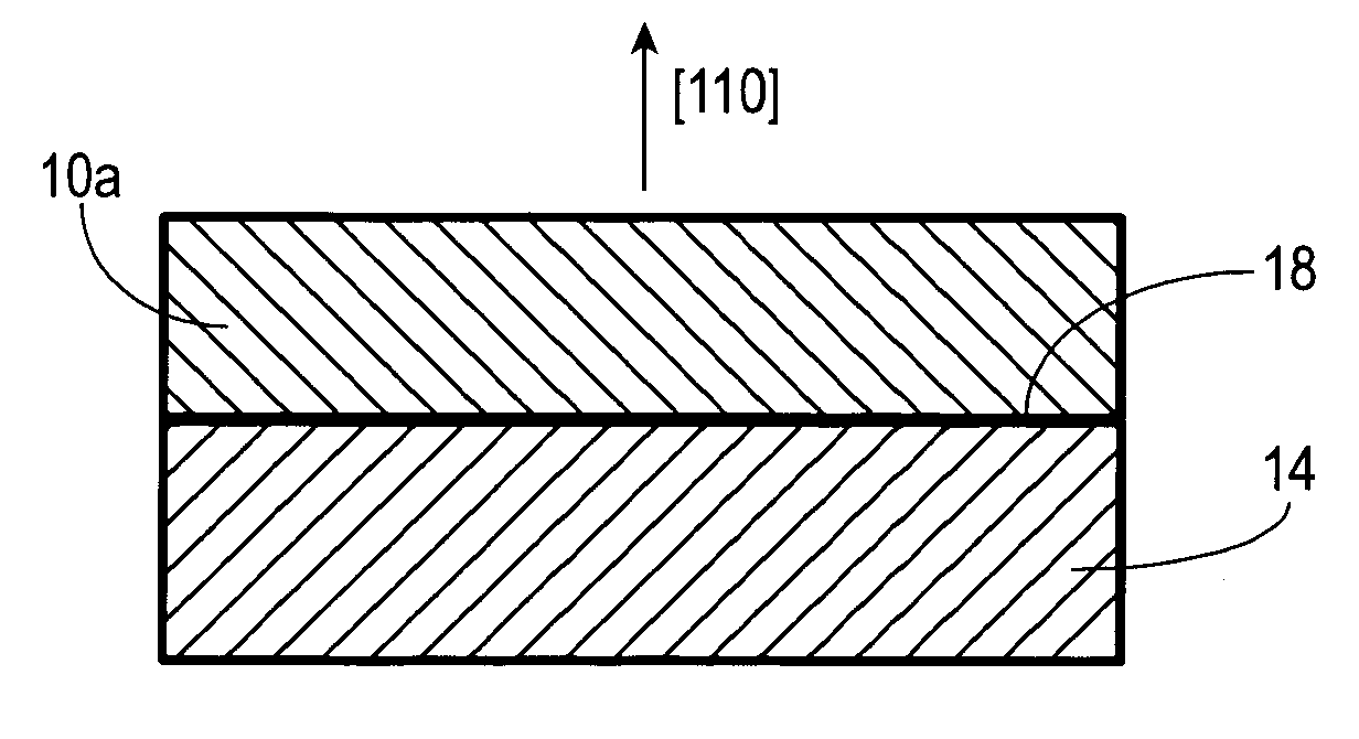
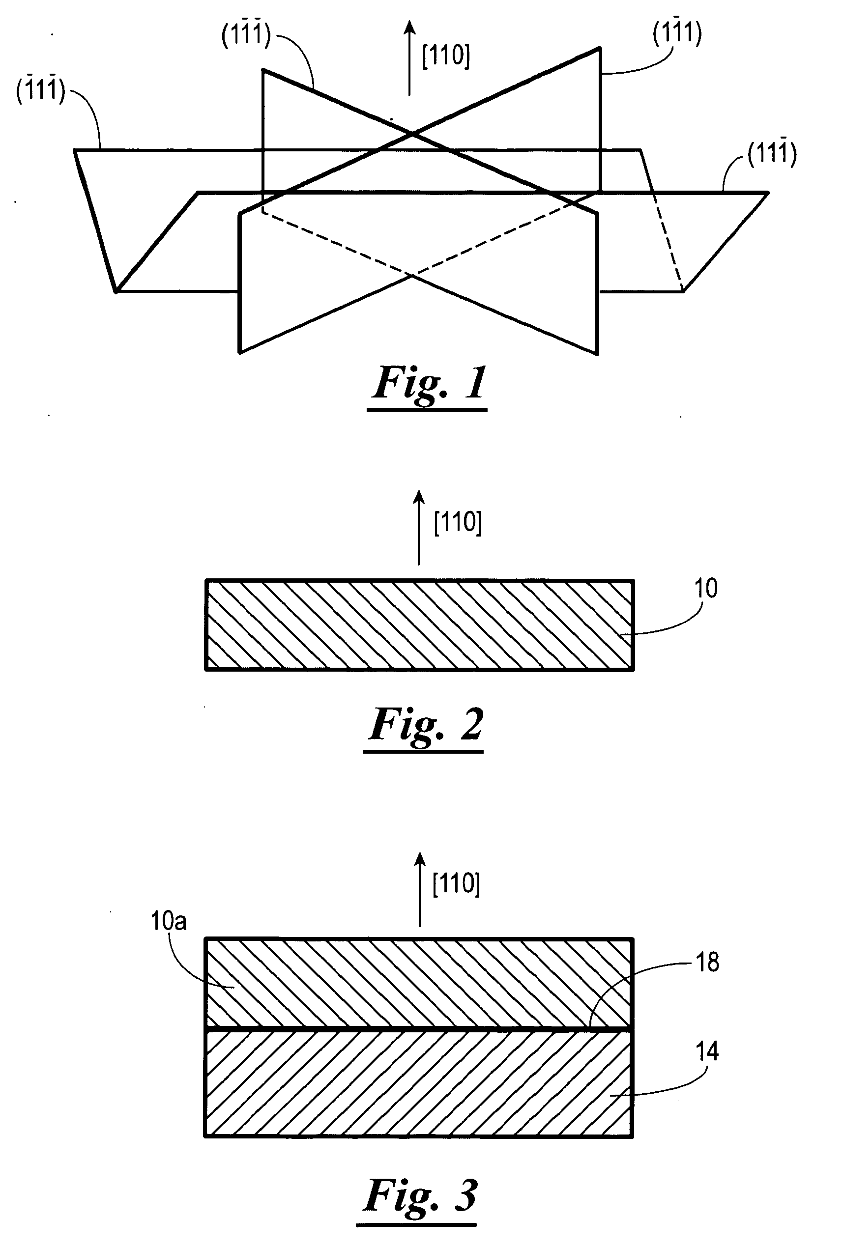
[0024] Generally, the present invention relates to a IV-VI group semiconductor structure having a [110] orientation, and a method for making and using the same. The [110] orientation of the group IV-VI semiconductor structure of the present invention offers some advantages over other orientations. Shown in FIG. 1 is a schematic representation of the geometry of [110] surfaces in a diamond cubic semiconductor material with the {111} planes shown. For example, a IV-VI lead salt semiconductor material having a rock salt structure would belong to the diamond cubic group. Also, shown in Table 1 below is the effective mass for different orientations for the energy minima shown in FIG. 1. For PbSe, ml≈2mt.

TABLE 1Effective masses along differentorientations for L-valley energy minimaSurfaceOrientationmxmymzDegeneracy{100}mt+2⁢ml33⁢mt⁢mlmt+2⁢ml4{110}mtml+2⁢mt33⁢mt⁢mlml+2⁢mt2mtmlml2{111}mtml1mtmt+8⁢ml99⁢mt⁢mlmt+8⁢ml3

[0025] The [110] orientation of the group IV-VI semiconductor structure of ...


PUM

PropertyMeasurementUnit
thicknessaaaaaaaaaa
thicknessaaaaaaaaaa
semiconductoraaaaaaaaaa

Abstract

A method of growing and fabricating a group IV-VI semiconductor structure, for use in fabricating devices. In one embodiment, the group IV-VI semiconductor structure produced by the method of the present invention includes a group IV-VI material grown on a selected orientation of [110]. The devices fabricated can be a laser, detector, solar cell, thermal electrical cooling devices, etc. A laser device produced according to the present method will have a low threshold due to the lift-off of the energy degeneracy and low defect density. Growth on the [110] orientation also allows epitaxial growth of the semiconductor structure on a dissimilar substrate, which could improve the thermal dissipation and thus increase the operating temperature of the laser device.

Description

CROSS-REFERENCE TO RELATED APPLICATIONS [0001] The present application claims priority to the provisional patent application identified by the U.S. Ser. No. 60 / 542,023, which was filed on Feb. 5, 2004, the entire content of which is hereby expressly incorporated herein by reference.STATEMENT REGARDING FEDERALLY SPONSORED RESEARCH OR DEVELOPMENT [0002] Research regarding one or more portions of the present invention may have been funded pursuant to DOD ARO Grant Number DAAD19-03-1-0313.BACKGROUND OF THE INVENTION [0003] IV-VI lead salt semiconductors have wide spread applications for devices such as mid-infrared lasers, detectors and thermal electrical cooling devices. Previously, these devices have been fabricated using either [100] or [111] substrates such as [100] IV-VI substrates, [111] BaF2 substrates and [111] Si substrates. Efforts have also been made to fabricate devices on III-V GaAs, GaSb substrates and II-VI CdTe, CdSe substrates. [0004] In the area of lasers, much of the ...

Claims


Application Information

Patent Timeline
Patent Type & Authority Applications(United States)
IPC IPC(8): H01L29/00H01L47/00H01S5/32
CPCH01S5/3222H01L31/0324
Inventor SHI, ZHISHENG
Owner THE BOARD OF RGT UNIV OF OKLAHOMA
Why Eureka
Try Eureka