

Light-emitting device and method of manufacturing the same
a technology of light-emitting devices and manufacturing methods, which is applied in the direction of semiconductor devices, electrical devices, basic electric elements, etc., can solve the problems of difficult to improve the light extraction efficiency and disadvantageous reflection of light on the interface between the transparent substrate and the semiconductor element layer, and achieve the effect of improving the light extraction efficiency
- Summary
- Abstract
- Description
- Claims
- Application Information
AI Technical Summary
Benefits of technology
Problems solved by technology
Method used
Image

Examples
first embodiment
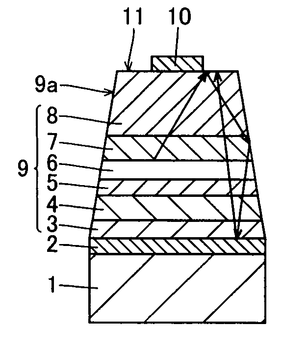
[0055] The structure of a nitride-based semiconductor light-emitting diode device according to a first embodiment of the present invention is described with reference to FIG. 1. Referring to FIG. 1, arrows denote paths of light.
[0056] In the nitride-based semiconductor light-emitting diode device according to the first embodiment, a conductive support substrate 1 is set on a side opposite to a light emission surface 11, as shown in FIG. 1. The conductive support substrate 1 consists of a semiconductor, a metal or a conductive resin film or a composite material of a metal and a metal oxide. The semiconductor used for the support substrate 1 may be prepared from a cleavable semiconductor such as Si, SiC, GaAs or ZnO. The metal used for the support substrate 1 is prepared from Al, Fe—Ni or Cu—W. The conductive resin film used for the support substrate 1 is prepared from a conductive resin film containing conductive particles of a metal or the like dispersed therein. The composite mate...
second embodiment
[0079] Referring to FIG. 9, inclined side surfaces 29a of a nitride-based semiconductor element layer 29 and a light emission surface 31 form an acute angle while lateral reflecting films are provided on the inclined side surfaces 29a of the nitride-based semiconductor element layer 29 in a nitride-based semiconductor light-emitting diode device according to a second embodiment of the present invention, dissimilarly to the aforementioned first embodiment. Referring to FIG. 9, arrows denote paths of light.
[0080] In the nitride-based semiconductor light-emitting diode device according to the second embodiment, an n-side electrode 22 of Al having a thickness of about 2 nm is formed on a conductive support substrate 21 set on a side opposite to the light emission surface 31, as shown in FIG. 9. The n-side electrode 22 is an example of the “reflecting film” in the present invention.
[0081] An n-type contact layer 23 of n-type GaN doped with Si having a thickness of about 0.5 μm is forme...
third embodiment
[0100] Referring to FIG. 19, inclined side surfaces 59a of a nitride-based semiconductor element layer 59 and a light emission surface 61 form an obtuse angle while the light emission surface 61 is corrugated in a nitride-based semiconductor light-emitting diode device according to a third embodiment of the present invention, dissimilarly to the aforementioned first and second embodiments.
[0101] In the nitride-based semiconductor light-emitting diode device according to the third embodiment, a p-side electrode 52 having a composition and a thickness similar to those of the p-side electrode 2 in the aforementioned first embodiment is bonded to a conductive support substrate 51 set on a side opposite to the light emission surface 61, as shown in FIG. 19. The p-side electrode 52 is an example of the “reflecting film” in the present invention.
[0102] A p-type contact layer 53 of p-type GaN doped with Mg having a thickness of about 0.2 μm is formed on the p-side electrode 52. This p-typ...
PUM
 Abstract
Description
Claims
Application Information