Optimized trench power MOSFET with integrated schottky diode

a technology of schottky diodes and trench power mosfets, which is applied in the direction of diodes, semiconductor devices, electrical equipment, etc., can solve the problems of high junction leakage of schottky interfaces, power loss, switching frequency, current drive capability and cost, etc., and achieve the effect of improving the efficiency of schottky interfaces

Inactive Publication Date: 2005-09-15
SEMICON COMPONENTS IND LLC
View PDF99 Cites 69 Cited by
  • Summary
  • Abstract
  • Description
  • Claims
  • Application Information

AI Technical Summary

Benefits of technology

[0005] In accordance with the present invention, a monolithically integrated structure combines a field effect transistor and a Schottky structure in an active area of a semiconductor substrate. The field effect transistor includes a first trench extending into the substrate and substantially filled by conductive material forming a gate electrode of the field effect transistor. A pair of doped source regions are positioned adjacent to and on opposite sides of the trench and inside a doped body region. The Schottky structure inc

Problems solved by technology

Power loss, switching frequency, current drive capability and cost are only few of the parameters that require optimization for a competitive mobile application.
This method requires special processing steps, and arriving at an optimal profile in practice while minimizing the penalty of adverse affects on other parameters can be a challenge in the sub-micron regime.
The higher junction leakage of the Schottky interface is however a drawback.
A drawback of the use of two discrete devices is the pa

Method used


Image

  • Optimized trench power MOSFET with integrated schottky diode
  • Optimized trench power MOSFET with integrated schottky diode
  • Optimized trench power MOSFET with integrated schottky diode

Examples


Embodiment Construction

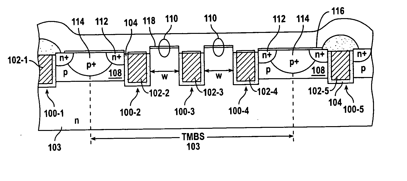
[0024] In accordance with the present invention a trench power MOSFET includes a Schottky structure which consumes about 2.5% to 5% of the total active area while the field effect transistor consumes the remaining portion of the active area. It has been discovered that this results in the most optimum device efficiency. In one particular application, the loss contribution of the low-side switch of a DC-DC converter is substantially reduced when the power MOSFET device of the present invention is used as the low-side switch. The phrases “Schottky structure” and “trench MOS barrier Schottky (TMBS)” are used interchangeably in the specification and the drawings.

[0025]FIG. 1 shows a cross-sectional view of a simplified example of an integrated trench MOSFET-Schottky diode structure fabricated on a silicon substrate 103. A plurality of trenches 100 are patterned and etched into substrate 103. Substrate 103 may comprise an upper n-type epitaxial layer (not shown). A thin dielectric layer...


PUM


Abstract

In accordance with the present invention, a monolithically integrated structure combines a field effect transistor and a Schottky structure in an active area of a semiconductor substrate. The field effect transistor includes a first trench extending into the substrate and substantially filled by conductive material forming a gate electrode of the field effect transistor. A pair of doped source regions are positioned adjacent to and on opposite sides of the trench and inside a doped body region. The Schottky structure includes a pair of adjacent trenches extending into the substrate. Each of the pair of adjacent trenches is substantially filled by a conductive material which is separated from trench side-walls by a thin layer of dielectric. The Schottky structure consumes 2.5% to 5.0% of the active area, and the field effect transistor consumes the remaining portion of the active area.

Description

BACKGROUND OF THE INVENTION [0001] The present invention relates in general to semiconductor power device technology, and in particular to a semiconductor power device with a trenched gate MOSFET and Schottky diode integrated in an optimum manner, and its method of manufacture. Emerging portable applications are driving semiconductor performance from many aspects. Power loss, switching frequency, current drive capability and cost are only few of the parameters that require optimization for a competitive mobile application. In the DC-DC conversion area, the switching losses associated with both the high-side and low-side transistors in the chopper stage require careful design to minimize power loss. Device characteristics such as series gate resistance, gate capacitance, blocking capability, and the on state resistance are important considerations in the device design. [0002] Several approaches have been proposed for controlling the power losses. One approach tailors the lifetime pro...

Claims


Application Information

Patent Timeline
IPC IPC(8): H01L29/80
CPCH01L29/0696H01L29/407H01L29/8725H01L29/7813H01L29/7806
Inventor CALAFUT, DANIELREXER, CHRISTOPHER L.
Owner SEMICON COMPONENTS IND LLC
Why Eureka
Try Eureka