Contact structure for nanometer characteristic dimensions

Inactive Publication Date: 2005-09-15
TAIWAN SEMICON MFG CO LTD
View PDF8 Cites 40 Cited by
  • Summary
  • Abstract
  • Description
  • Claims
  • Application Information

AI Technical Summary

Benefits of technology

[0008] To achieve the foregoing and other objects, and in accordance with the purposes of the present invention, as embodied and broadly described herein, the pre

Problems solved by technology

The decreasing characteristic dimensions of integrated circuits creates a host of new processing problems as well as design problems which must be overcome to successfully achieve higher levels of integration.
For example, as characteristic dimensions of transistor devices are scaled down to deep submicron dimensions, the contact opening width allowable is increasing limited due to the shrinking size of the contact areas.
Conventional processing steps such as photolithography and reactive ion etching have increasingly limited process windows in order to make reliable contacts while the shor

Method used


Image

  • Contact structure for nanometer characteristic dimensions
  • Contact structure for nanometer characteristic dimensions
  • Contact structure for nanometer characteristic dimensions

Examples


Example

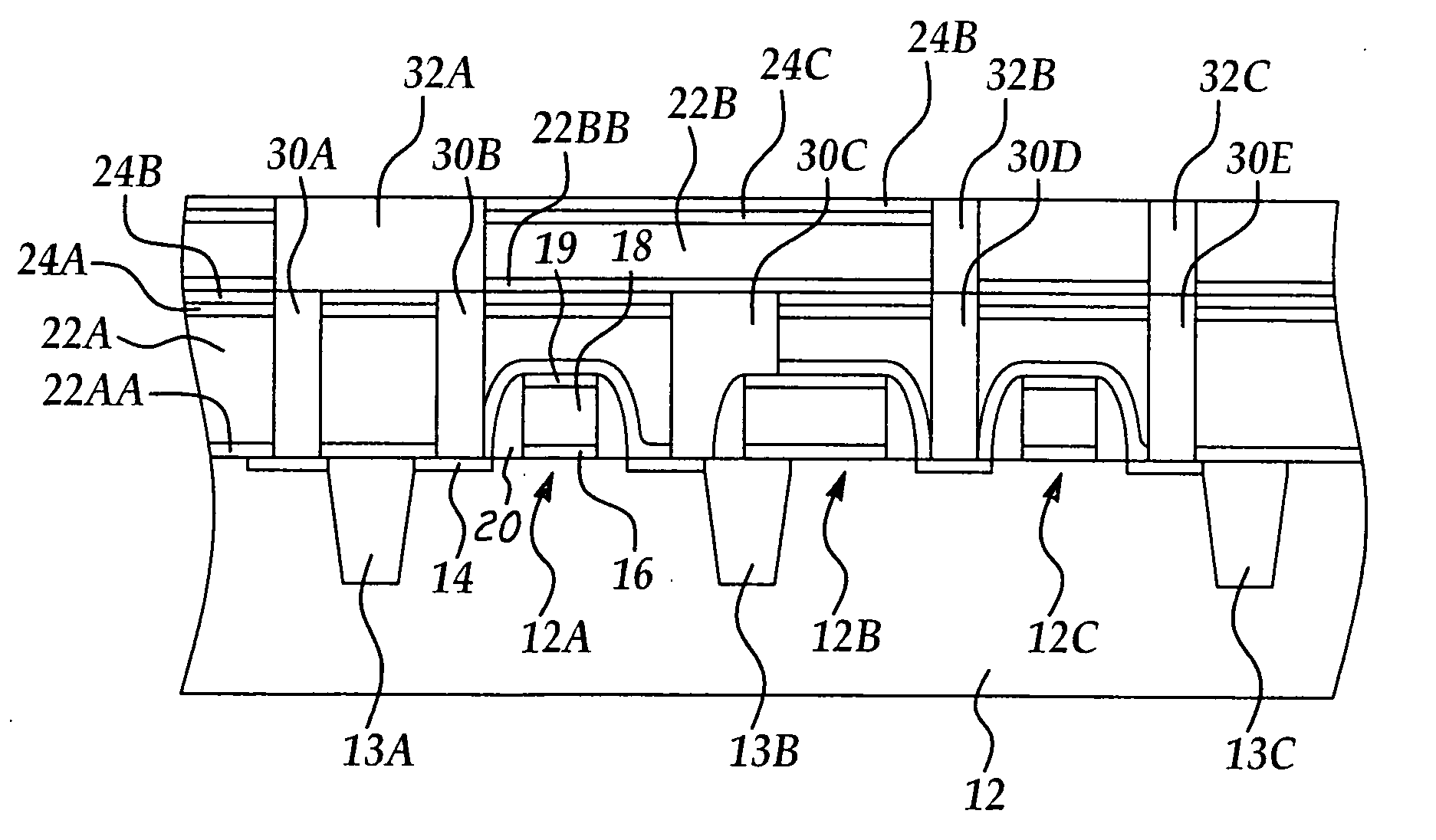
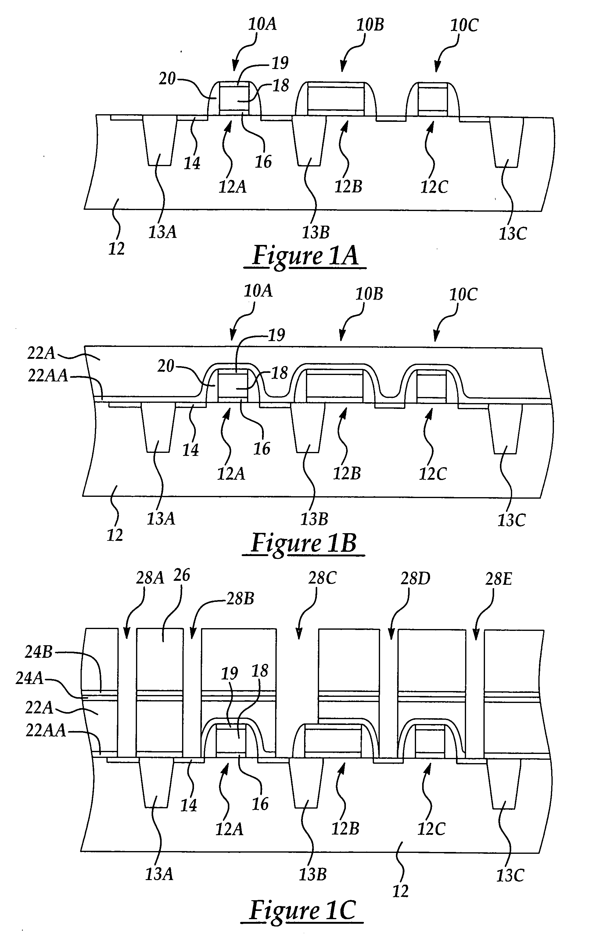
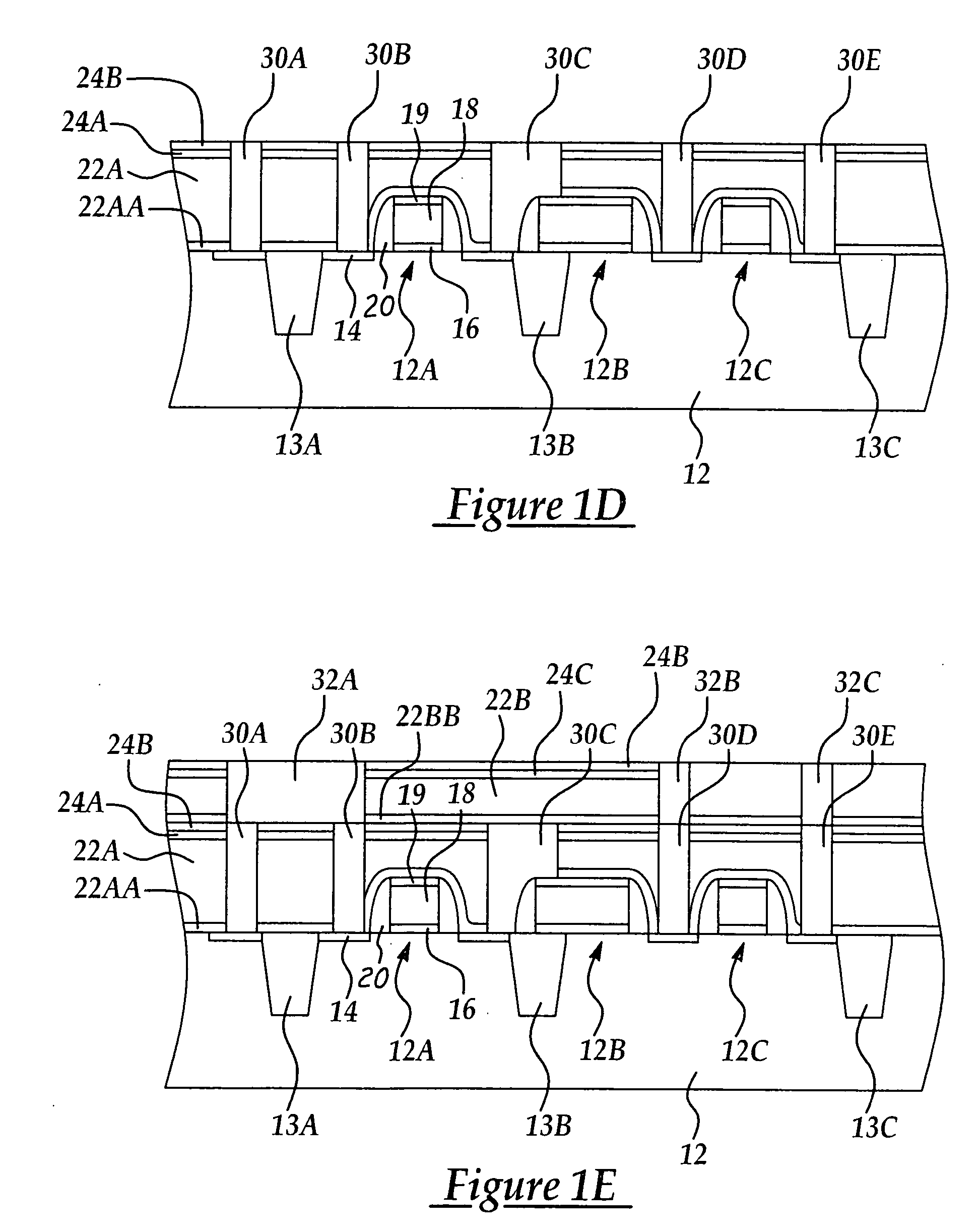
[0013] Although the method of the present invention is explained with reference to an exemplary CMOS transistor and shallow trench isolation (STI) structures, it will be appreciated that the shallow contact interconnects and method of forming the same may be applied in general to forming contact interconnects where an integrated circuit device or process may be improved by forming contact interconnects in a multi-step process to overcome processing issues and device performance issues related to forming high aspect ratio damascene openings. In addition, it will be appreciated that while the device and method of the present invention is particularly advantageously used for forming integrated circuit devices with characteristic dimensions (e.g., gate lengths) less than about 60 nm, including less than about 45 nm, that the method and structure may be used in forming larger characteristic dimension devices.

[0014] Referring to FIGS. 1A-1E in an exemplary embodiment of the method of the...


PUM


Abstract

A contact interconnect structure including the method of providing a semiconductor substrate including CMOS devices including active contact regions; forming a first set of dielectric layers to form a first thickness for etching a first set of openings through a thickness thereof including a bottom portion having a maximum width of less than about 70 nanometers; etching the first set of openings to contact active contact regions; filling the first set of openings with a first metal; forming a second set of dielectric layers to form a second thickness for etching a second set of openings through the second thickness comprising a bottom portion having a maximum width of less than about 70 nanometers; etching the second set of openings to provide electrical communication with the first set of openings; and, filling the second set of openings with a second metal to form contact interconnects.

Description

FIELD OF THE INVENTION [0001] This invention generally relates to formation of nanometer scaled CMOS integrated circuits and more particularly to contact interconnect structures and method for forming the same to achieve reliable electrical contacts including to active contact regions in CMOS integrated circuits. BACKGROUND OF THE INVENTION [0002] Increasingly, integrated circuits require a higher density of device integration with increasingly shrinking characteristic dimensions, such dimensions referred to as deep sub-micron or nanometer technology where characteristic (critical) dimensions such as gate length are expected to soon decrease below 60 nm as well as below 45 nm. The decreasing characteristic dimensions of integrated circuits creates a host of new processing problems as well as design problems which must be overcome to successfully achieve higher levels of integration. [0003] Contact interconnects, also referred to as vias, are particularly critical for making contact ...

Claims


Application Information

Patent Timeline
IPC IPC(8): H01L23/48
CPCH01L21/76895H01L21/76801H01L21/76816H01L2924/00013H01L2224/13099H01L2224/05099H01L2224/13599H01L2224/05599H01L2224/29099H01L2224/29599
Inventor LIAW, JHON JHY
Owner TAIWAN SEMICON MFG CO LTD
Why Eureka
Try Eureka