Solid-state image sensor for improving sensing quality and manufacturing method thereof
- Summary
- Abstract
- Description
- Claims
- Application Information
AI Technical Summary
Benefits of technology
Problems solved by technology
Method used
Image
Examples
Embodiment Construction
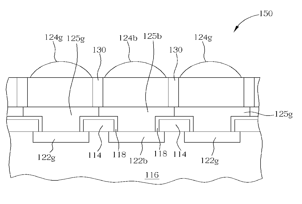
[0017] Please refer to FIG. 4, which shows a cross-sectional view of an image sensor 100 according to the present invention. The image sensor 100 comprises a plurality of sensing units arranged in a Bayer pattern color filter array shown in FIG. 2. For simplicity, only a green sensing unit 102g and a blue sensing unit 102b are drawn and labeled. Photosensor elements 122b, 122g formed on the silicon substrate 116 are used for performing photoelectrical transformation. An insulating layer 106 made of SiO2 is formed on the substrate 116 by using a thermal oxidation process or a chemical vapor deposition (CVD). Each sensing unit 102b, 102g includes a transfer electrode (serving as a transfer transistor) 114b, 114g over the substrate 116, (i.e. on the insulating layer 106) and respectively coupled to photosensor elements 122b, 122g. The transfer electrodes 114b, 114g are used for transferring electrical signals from the photosensor elements 122b, 122g. In addition, each sensing unit 102b...
PUM
 Abstract
Description
Claims
Application Information


