

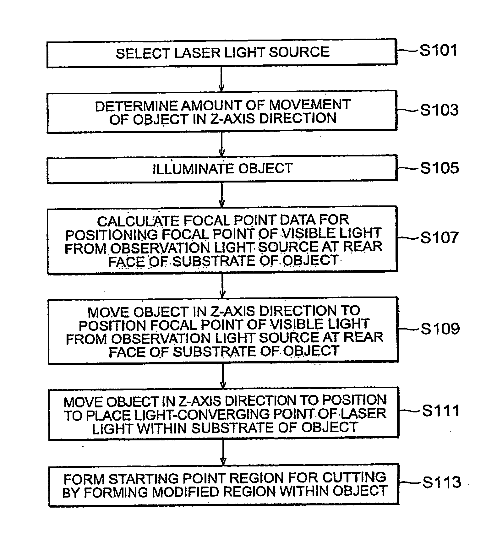
Laser processing method
a laser processing method and laser technology, applied in glass making apparatus, manufacturing tools, welding/soldering/cutting articles, etc., can solve the problems of glass substrate gap and possible cutting failure, and achieve the effect of small force and high accuracy
- Summary
- Abstract
- Description
- Claims
- Application Information
AI Technical Summary
Benefits of technology
Problems solved by technology
Method used
Image

Examples
example 1
[0128]FIG. 16A is a view showing a case where a modified region 7 is formed near the rear face of a substrate 15 in the object to be processed 1 in accordance with Example 1, whereas FIG. 16B is a view showing a case where a modified region 7 is formed near the front face of the substrate 15 in the object 1 in accordance with Example 1. Examples of the object 1 shown in FIGS. 16A and 16B include one used for next-generation high-speed / low-power-consumption devices and one for next-generation devices.
[0129] The substrate 15, first laminate part 17a, and second laminate part 17b for a next-generation high-speed / low-power-consumption device are Si (500 μm), SiO2 (1 μm), and Si (3 μm respectively. On the other hand, the substrate 15, first laminate part 17a, and second laminate part 17b for a next-generation device are Si(500 μm), SrTiO3 (several hundred μm), and GaAs (several hundred μm), respectively (where values in parentheses indicate thickness).
[0130] When the modified region 7 ...
example 2
[0132]FIG. 17A is a view showing a case where a modified region 7 is formed near the rear face of a substrate 15 in the object to be processed 1 in accordance with Example 2, whereas FIG. 17B is a view showing a case where a modified region 7 is formed near the front face of the substrate 15 in the object 1 in accordance with Example 2. The object 1 shown in FIGS. 17A and 17B is one for a blue LD / LED, examples of its substrate 15 / laminate part 17 include Al2O3 (500 μm) / a laminated functional film (several hundred nm) in which a plurality of layers of semiconductor crystals such as GaN are formed, and Al2O3 (500 μm) / a laminated functional film (several hundred nm) in which a plurality of layers such as a ZnO layer are formed (where values in parentheses indicate thickness).
[0133] When the modified region 7 is positioned near the rear face 21 of the object 1, the knife edge 23 is pressed against the front face 3 of the object 1 as shown in FIG. 17A, so as to break and cut the object ...
example 3
[0134]FIG. 18A is a view showing a case where respective modified regions 7 are formed near the front face of a substrate 15 and in a laminate part 17 in the object to be processed 1 in accordance with Example 3; FIG. 18B is a case where a modified region 7 is formed near the rear face of the substrate 15 in the object 1 in accordance with Example 3; and FIG. 18C is a view showing a case where a modified region 7 is formed near the front face of the substrate 15 in the object 1 in accordance with Example 3. The object 1 shown in FIGS. 18A to 18C is one for an infrared light detecting device, examples of its substrate 15 / laminate part 17 include Al2O3 (500 μm) / PbSe (10 μm), and Al2O3 (500 μm) / HgCdTe (10 μm) (where values in parentheses indicate thickness).
[0135] When the modified region 7 is positioned near the front face 3 of the object 1 as shown in FIGS. 18A and 18C, the knife edge 23 is pressed against the rear face 21 of the object 1, so as to break and cut the object 1, from t...
PUM
| Property | Measurement | Unit |
|---|---|---|
| Moving speed | aaaaa | aaaaa |
| thickness | aaaaa | aaaaa |
| thickness | aaaaa | aaaaa |
Abstract
Description
Claims
Application Information