
Defect inspection apparatus

a technology of inspection apparatus and defective parts, which is applied in the direction of photomechanical equipment, instruments, nuclear engineering, etc., can solve the problems of low inability to display which region of the sample under test, and inspection apparatus cannot display the defective sample. , to achieve the effect of improving the utilization efficiency of hardware and softwar

Inactive Publication Date: 2005-09-22
EBARA CORP
View PDF5 Cites 48 Cited by
  • Summary
  • Abstract
  • Description
  • Claims
  • Application Information

AI Technical Summary

Benefits of technology

[0016] The present invention has been made in view of the problems stated above inherent to the prior art, and a first object thereof is to improve utilization efficiencies of hardwares and softwares in a defect inspection apparatus in which a plurality of inspection algorithms are selectively executed
[0017] A second object of the present invention is to provide a defect inspection apparatus which is capable of displaying on a monitor so far a scanned region of a sample such as a semiconductor wafer and defective spots in the scanned region during a defect inspection thereof, thereby permitting an operator to determine whether or not the sample currently under test passes or fail even in the middle of the inspection.
[0036] Since the prevent invention of the first aspect is constituted as described above, a plurality of inspection algorisms can be selectively performed using a hardware / software. In addition, two or more algorisms can be performed even on one wafer. Accordingly, utilization efficiencies of a hardware / software can be improved.
[0044] Since the defect inspection apparatus according to the present invention of the second aspect is constituted as stated above, an operator of the apparatus can monitor an image of a sample of a display and judge whether the sample under inspection contains a defect(s) even during a continuation of the sample inspection. If a sample is determined to be defect even at a middle of the inspection, the operator can stop the inspection and execute a next sample inspection. Therefore, a throughput of a defect inspection can be improved.
[0045] When a bi-directional scanning is executed, the defect inspection throughput can be further accelerated.

Problems solved by technology

Therefore, utilization efficiency of the hardwares and softwares is relatively low.
However, an apparatus which can display on a display device which samples have been inspected and whether each inspected sample passes or fails, is not capable of displaying in which region on a sample under test is being currently scanned, or at which location a defect is detected in a scanned region of the sample under test.
Therefore, even if a sample currently under test includes a large number of defects in a scanned region and is therefore determined as defective, the inspection apparatus cannot display that the sample is defective until the sample has gone through the test.
Generally, in a semiconductor wafer defect inspection, since it takes several hours to inspect a complete wafer, a challenge exists in reducing an inspection time period to improve the throughput of the defect inspection.
Nevertheless, a reduction in the inspection time period may degrade inspection accuracy.

Method used


Image

  • Defect inspection apparatus
  • Defect inspection apparatus
  • Defect inspection apparatus

Examples


Embodiment Construction

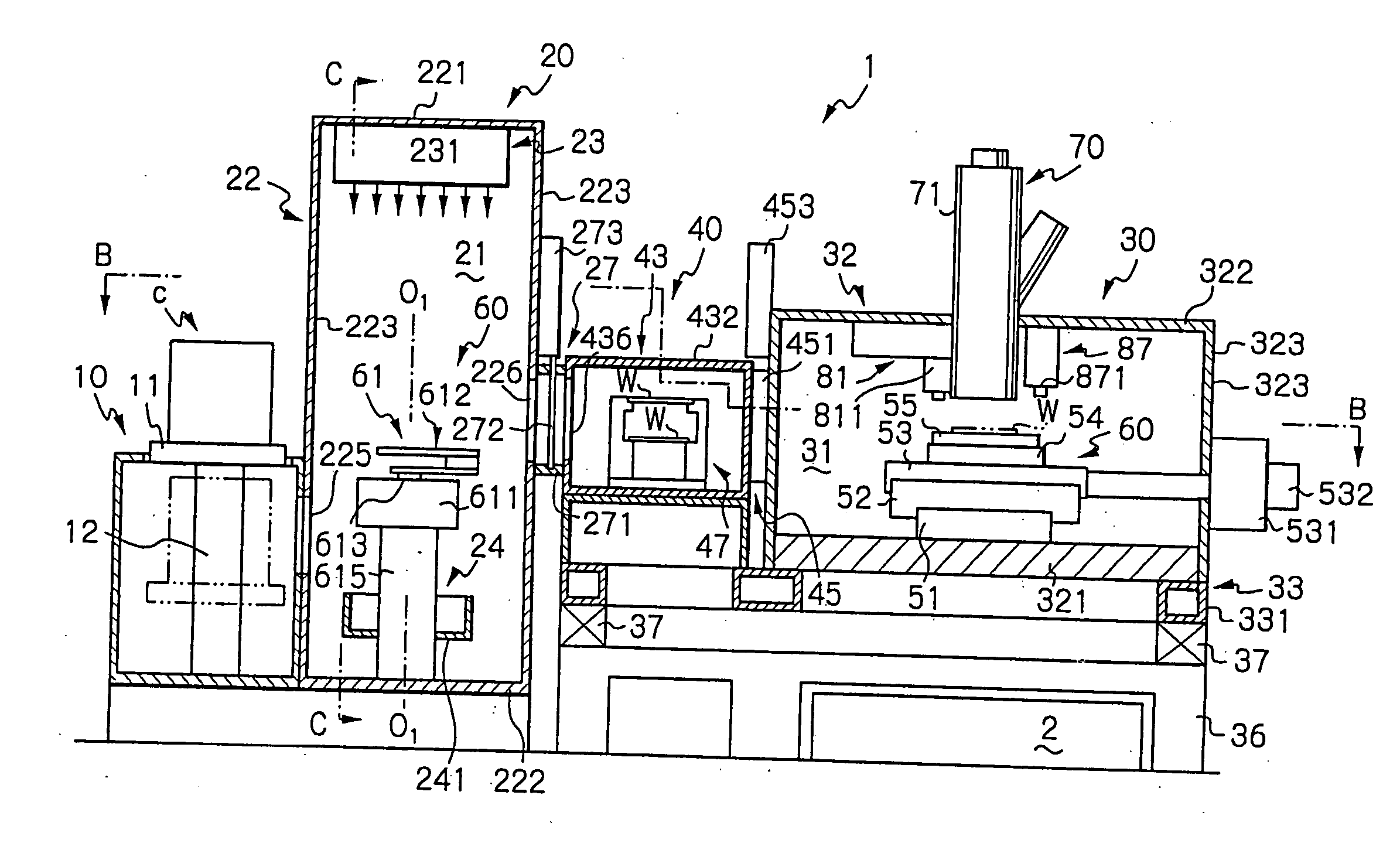
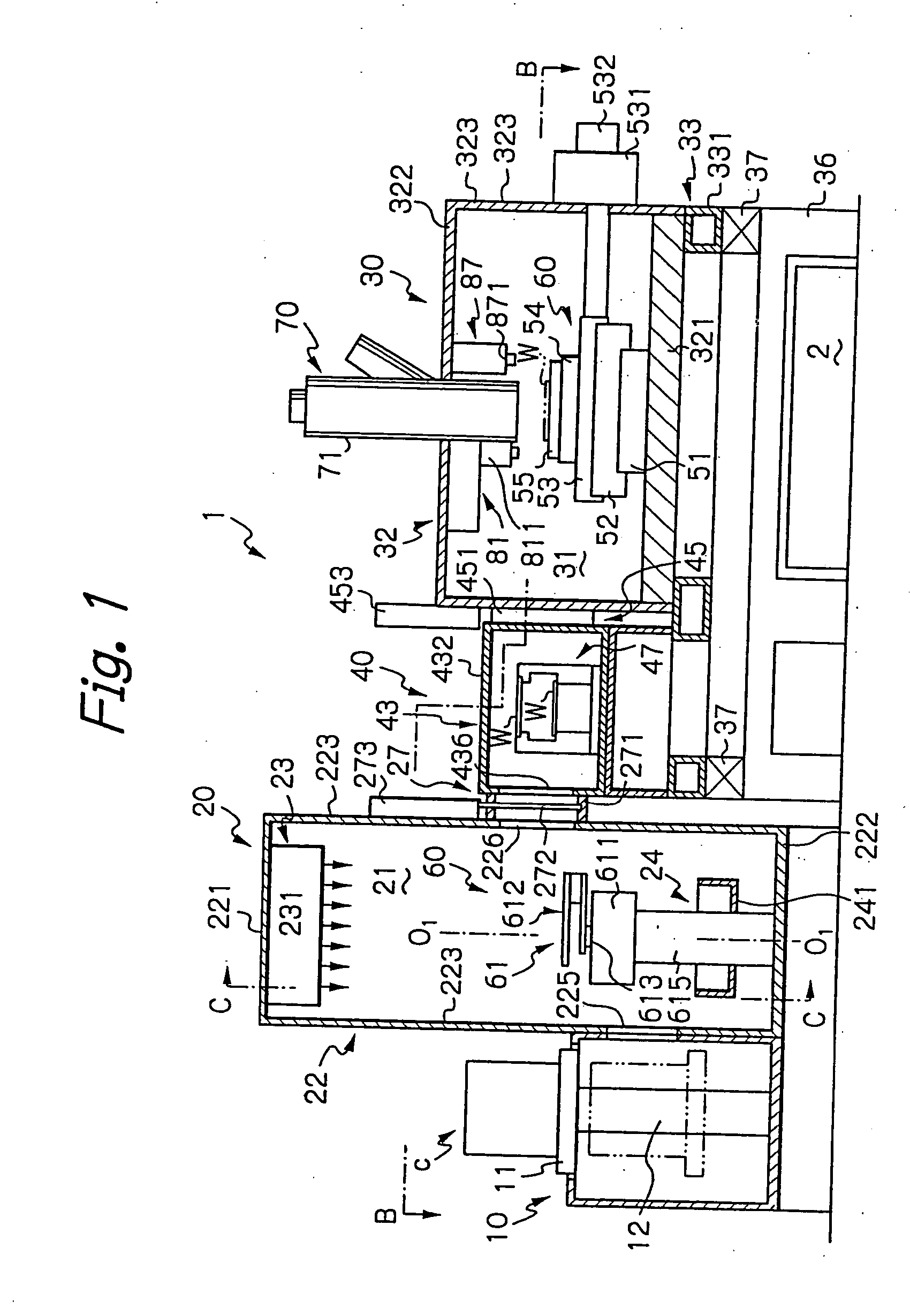
[0077] Before describing preferred embodiments of a defect inspection apparatus according to the present invention, description will be made of the general configuration of a semiconductor wafer inspection system which can incorporate and utilize the defect inspection apparatus according to the present invention.

[0078]FIG. 1 and 2 are an elevation and a plan view illustrating main components of the inspection system 1, respectively. The inspection system 1 comprises a cassette holder 10 for holding a cassette which contains a plurality of wafers; a mini-environment device 20; a main housing 30; a loader housing 40 disposed between the mini-environment device 20 and the main housing 30 for defining two loading chambers; a stage device 50 disposed within the main housing 30 for carrying a wafer W for movements; a loader 60 for loading a wafer from the cassette holder 10 onto the stage device 50 disposed within the main housing 30; and an opto-electro system 70 mounted in the main hou...


PUM


Abstract

A controller determines, in response to a position coordinate from an X / Y interferometer, which algorism should be used for current inspection, and controls a connection status of a switch to store a reference image corresponding thereto in an image memory. The reference image is one of an image of a sample surface obtained by an image data acquisition unit, an image provided from a cell reference image generation unit, and an image provided from a CAD data reference image generation unit. The controller further controls a connection status of a second switch to provide the reference image associated with the current inspection algorism to an image comparator, where the provided reference image is compared with a currently obtained image. On the basis of a result of the comparison, a defect determination unit determines the presence / absence of a defect. Therefore, an utilization efficiency of a defect inspection apparatus which is capable of performing a plurality of defect inspection algorism, can be improved.

Description

BACKGROUND OF THE INVENTION [0001] The present invention relates to a defect inspection apparatus for inspecting a sample formed with a pattern on the surface thereof to detect defects, and more particularly, to a defect inspection apparatus which irradiates a sample such as a wafer with an electron beam in a semiconductor manufacturing process, captures secondary electrons and the like, which vary depending on the nature of the surface of the sample, to form image data, and evaluates defects on the pattern and the like on the sample surface on the basis of the image data at a high throughput. [0002] In semiconductor manufacturing processes, design rules is about to enter a 100-nm era, and the manufacturing form is shifting from mass manufacturing of one type of product, as represented by DRAM (dynamic random access memory), to flexible (or multiple types and small amount) manufacturing such as SOC (silicon on chip). This shift is accompanied by an increased number of manufacturing ...

Claims


Application Information

Patent Timeline
IPC IPC(8): G01N21/956G03F7/20G21K7/00
CPCG01N21/95607G03F7/7065H01J2237/2487H01J37/265H01J37/222
Inventor KIMBA, TOSHIFUMI
Owner EBARA CORP
Learn More