Image display apparatus using thin-film transistors

a technology of thin-film transistors and display apparatuses, which is applied in the direction of identification means, tableware, instruments, etc., can solve the problems of difficult computer use in such a way, noise in external apparatuses, and unsatisfactory electromagnetic radiation from transmission lines, and achieve high-quality image display and low cost

Inactive Publication Date: 2005-09-22
SHARP KK
View PDF3 Cites 21 Cited by
  • Summary
  • Abstract
  • Description
  • Claims
  • Application Information

AI Technical Summary

Benefits of technology

[0019] According to the embodiments of the present invention, it is possible to realize a flat display at low cost, which can effect high-quality image display even in a mobile environment in which a sufficient transmission capacity is not always secured.

Problems solved by technology

If the frequency of the transmission line 144 increases, there arises such a problem that undesirable electromagnetic radiation occurs from the transmission line and noise is produced in the external apparatus due to electromagnetic interference (EMI).
It is thus difficult to use the computer in such a way that the light-weight display apparatus alone is moved and made to display an image at a place where image display needs to be performed.
This type of display apparatus, however, is not adaptable to such a future ubiquitous computing environment that computers are used anywhere, anytime.
The anywhere, anytime use means that the transmission line with a sufficient performance is not always secured.
As stated above, there is such a problem that the display apparatus 100 that requires a very high clock frequency for transmitting bitmap data is not easily adaptable to the environment, such as a wireless transmission system, where a sufficient transmission capacity is not always secured.

Method used


Image

  • Image display apparatus using thin-film transistors
  • Image display apparatus using thin-film transistors
  • Image display apparatus using thin-film transistors

Examples


first embodiment

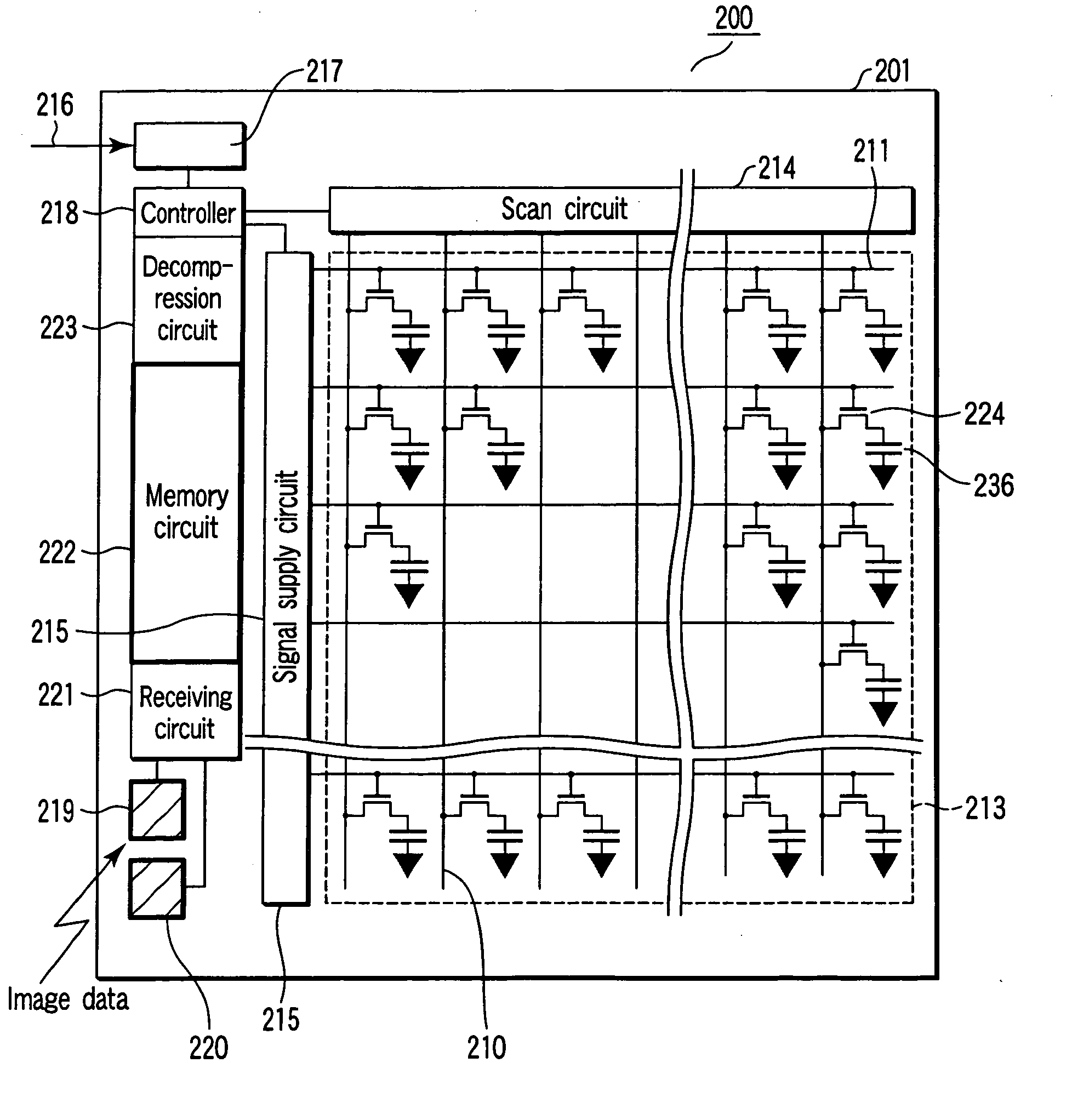
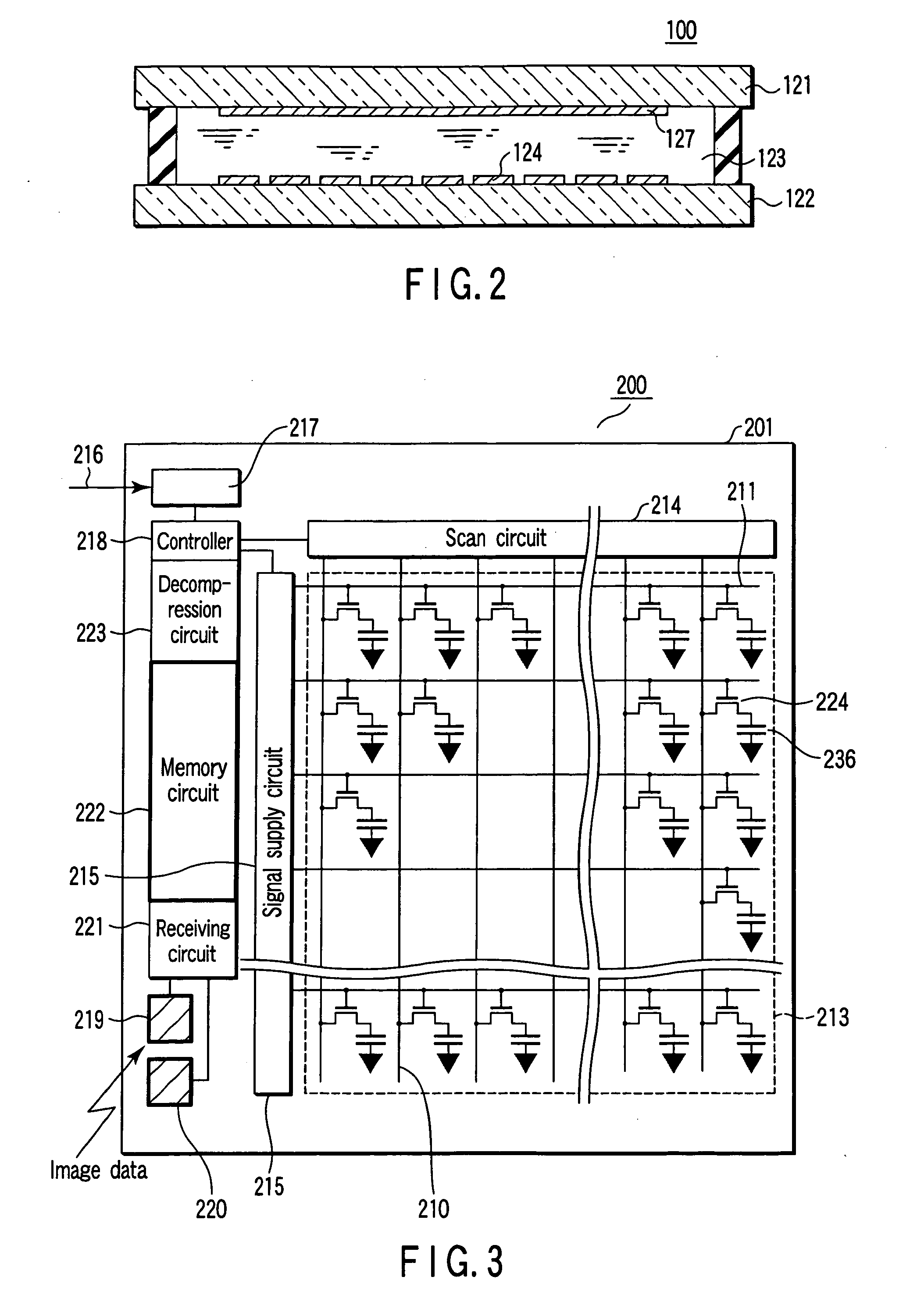
[0054]FIG. 3 shows a display substrate 200 of a display apparatus according to a first embodiment of the present invention. This display apparatus is a so-called active matrix display apparatus. A glass substrate 201 in FIG. 3 corresponds to the transparent substrate 122 in FIG. 1. The glass substrate 201 is an improvement of the transparent substrate 122.

[0055] A plurality of scan lines 210 and a plurality of video signal lines 211 are arranged in a matrix on the insulating substrate 201, for example, a transparent no-alkali glass substrate 201. The substrate 201 is not limited to the glass substrate, and may be a quartz substrate or a plastic substrate. A thin-film transistor active matrix region 213 is formed such that a plurality of thin-film transistors (TFTs) 224 are disposed in rectangular pixel regions that are defined by the lines 210 and 211. A scan circuit 214 and a signal supply circuit 215, which are formed using thin-film transistors, are disposed in order to drive th...

second embodiment

[0069]FIG. 8 shows the structure of an active matrix display apparatus according to a second embodiment of the present invention. The embodiment of FIG. 8 is characterized in that an inductor, which is formed, for example, by winding a metal thin film by a predetermined number of turns, is used as an element for receiving compressed image data from outside.

[0070] Like the embodiment of FIG. 3, a plurality of scan lines 210 and a plurality of video signal lines 211 are arranged in a matrix on a no-alkali glass substrate 201 that is an insulating substrate. Unlike the embodiment of FIG. 3, a thin-film transistor active matrix region 253 is formed such that two P-type thin-film transistors 250 and 251, a capacitance element 252 and a pixel 256 are disposed in each of a plurality of rectangular pixel regions that are defined by the lines 210 and 211. A scan circuit 254 and a signal supply circuit 255, which are formed using thin-film transistors, are disposed in order to drive the thin...

third embodiment

[0079]FIG. 10 is a perspective view that shows a display substrate 200 and a working table 264 of the system apparatus, according to a third embodiment of the present invention.

[0080] In the present embodiment, the display apparatus 200 includes, like the second embodiment, a inductive-coupling non-contact transmission line. A receiving inductor element 259 for forming the non-contact transmission line is provided on the display substrate 200. On the other hand, the working table 264 having a larger area than the display substrate 200 is provided on the system substrate side. A transmission circuit 262 and a transmission inductor element 265 are formed on the working table 264. The working table 264 receives a necessary image signal from an external system apparatus (not shown) over a connection cable 263.

[0081] The working table 264 itself may be a separate display apparatus, and a system including a plurality of display apparatuses may be constituted along with the display subst...


PUM

PropertyMeasurementUnit
sizeaaaaaaaaaa
sizeaaaaaaaaaa
widthaaaaaaaaaa

Abstract

There are provided a display apparatus and a display method, with which compressed image data that is to be decompressed can be transmitted to the display apparatus in an environment in which a transmission capacity is not always secured, and good image display is realized. An example of the display apparatus is an active matrix display apparatus formed by using thin-film transistors formed on an insulating substrate. In the active matrix display apparatus, a circuit that receives an image data signal from an external system via a non-contact transmission path and amplifies the image data signal, a circuit that processes the image data signal, and a memory circuit that stores the processed image data are integrated on the insulating substrate.

Description

CROSS-REFERENCE TO RELATED APPLICATIONS [0001] This application is based upon and claims the benefit of priority from prior Japanese Patent Applications No. 2004-081310, filed Mar. 19, 2004; and No. 2004-366598, filed Dec. 17, 2004, the entire contents of both of which are incorporated herein by reference. BACKGROUND OF THE INVENTION [0002] 1. Field of the Invention [0003] The present invention relates to a structure of a display apparatus using thin-film transistors that are formed by making use of a crystalline semiconductor thin film that is formed on an insulating substrate. [0004] 2. Description of the Related Art [0005] An active-matrix flat-panel display using thin-film transistors is known as a display apparatus for OA equipment, etc., which displays image information and character information. In recent years, with a development of multi-media communication technology, a function-integrated display that is called “system-on-panel” has attracted attention as a next-generatio...

Claims


Application Information

Patent Timeline
Patent Type & Authority Applications(United States)
IPC IPC(8): G02F1/133G02F1/00G02F1/1362G09F9/00G09F9/30G09F9/33G09F9/35G09G3/20G09G3/30G09G3/32G09G3/36H01L21/84H01L27/12H01L51/50H04N1/41H05B33/14H05K1/02H05K1/11
CPCG02F1/13454G09G3/20G09G3/32G09G3/3648G09G2300/0426G09G2300/08H05K2201/10446H01L21/84H01L27/12H05K1/0239H05K1/0243H05K1/117H05K2201/10128G09G2330/06A47G21/103
Inventor KAWACHI, GENSHIROABE, HIROYUKIASADA, KUNIHIROIKEDA, MAKOTO
Owner SHARP KK
Why Eureka
Try Eureka