Intermediate substrate

a technology of intermediate substrate and substrate, which is applied in the direction of fixed capacitor details, fixed capacitors, printed circuit non-printed electric components association, etc., can solve the problems of difficult connection of each capacitor to an integrated circuit, noise propagation, and contrary to the current trend toward smaller devices, and achieves the effect of ensuring the stiffness of the intermediate substrate and sufficiently enduring thermal stress

Active Publication Date: 2005-09-22
NGK SPARK PLUG CO LTD
View PDF7 Cites 46 Cited by
  • Summary
  • Abstract
  • Description
  • Claims
  • Application Information

AI Technical Summary

Benefits of technology

[0009] An object of the present invention is to provide an intermediate substrate wherein, although a thin film capacitor is employed, the stiffness of the intermediate substrate is significantly improved and wherein, although a manufacturing proc

Problems solved by technology

When plural devices in the circuit block switch at high speeds at the same time, a large current is immediately induced from the power supply, so that a resultant deflection in the power supply voltage produces noise which propagates to the respective circuit blocks through the power lines.
Because of this, it is difficult to connect each capacitor to an integrated circuit containing a large number of densely packed terminals from the viewpoint of the corresponding installation demands.
Further, this approach is contrary to the current trend toward smaller size devices.
In high frequency operation (particularly at frequencies of 100 MHz or more) the above-mentioned problem with respect to noise due to a deflection in the power supply voltage is likely to occur at the time of high speed switching.
This is a problem because of the decrease in

Method used


Image

  • Intermediate substrate
  • Intermediate substrate
  • Intermediate substrate

Examples


Embodiment Construction

[0075] Hereinafter, various embodiments of the present invention will be described with reference to the accompanying drawings.

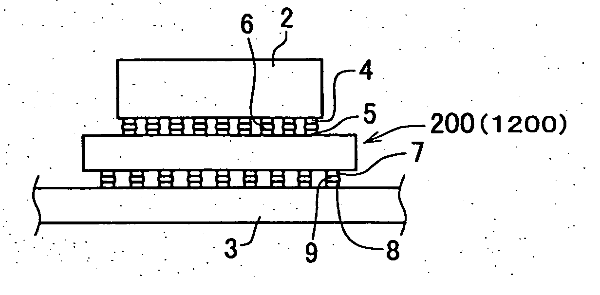
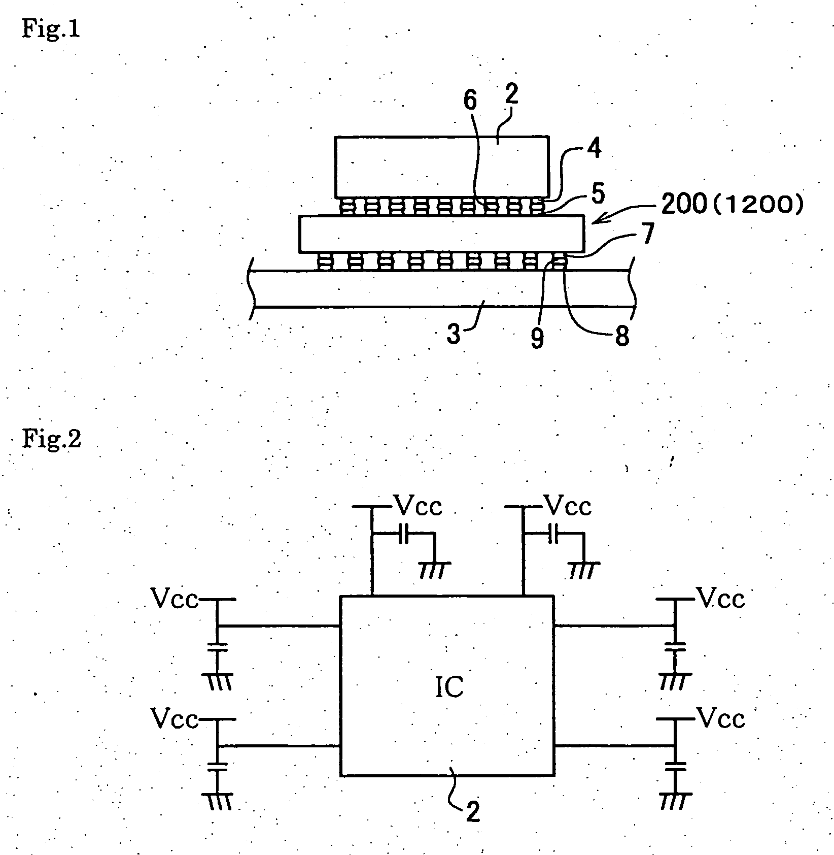
[0076]FIG. 1 shows an example in which an intermediate substrate 200 in accordance with a first embodiment of the present invention is constructed as an intermediate substrate disposed between a semiconductor integrated circuit device 2 and a main substrate 3. According to this embodiment, a first main surface of a sheet-like or substantially planar member is assumed to be a surface on the upper side as viewed. In FIG. 1 and a second main surface is assumed to be a surface on the lower side.

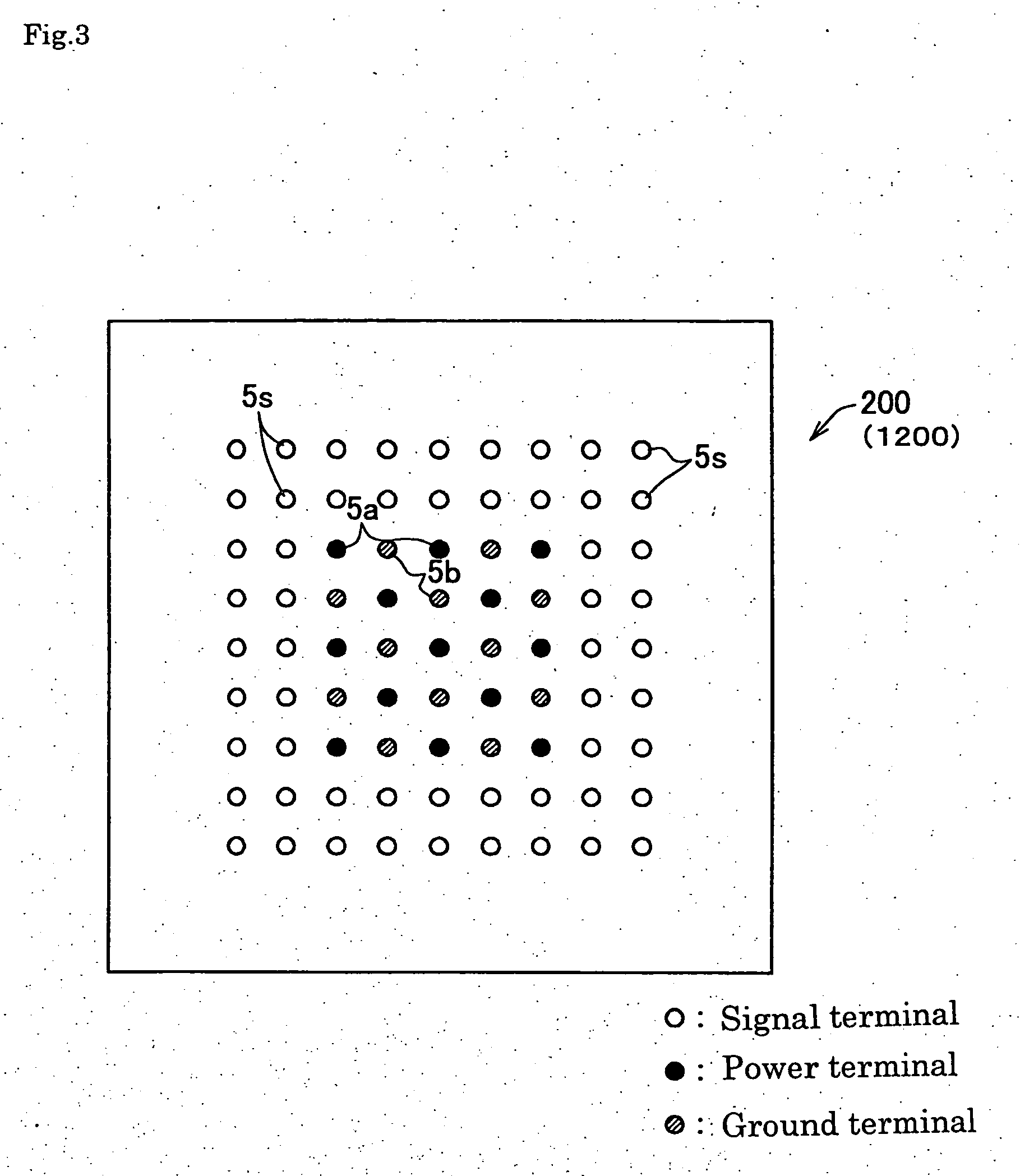
[0077] The semiconductor integrated circuit device 2 has a device side terminal array 4 comprising pluralities of signal terminals, power terminals and ground terminals on the second main surface, and is “flip chip” connected to a first terminal array 5 formed on the first main surface of the intermediate substrate 200 through a solder connection portion 6. On the other...


PUM


Abstract

An intermediate substrate includes a substrate core formed by a main core body portion constructed of a sheet of polymer material and having a subsidiary core accommodation portion formed therein. A ceramic subsidiary core portion, which is constructed of a ceramic sheet, is accommodated in the subsidiary core accommodation portion and is of a thickness matching that of the main core body portion. A thin film capacitor is formed on a first main surface side of a plate-like base of the core portion and includes first and second thin film electrodes separated from each other by a thin film dielectric layer so as to provide direct current isolation between the electrodes. First and second direct current isolated terminals of a first terminal array are electrically connected to the first and second thin film electrodes.

Description

BACKGROUND OF THE INVENTION [0001] 1. Field of the Invention [0002] The present invention relates to capacitors and, more particularly, to a capacitor formed as part of an intermediate substrate. [0003] 2. Description of Related Art [0004] Two prior art references of interest include a patent, Japanese Patent Application Laid-Open No. 2003-142624, and a publication entitled “Development of low inductance thin film decoupling capacitor,” Kazuaki Kurihara, Electronics installation technology, Vol. 19 (2003), No. 1, page 50. [0005] In integrated circuit devices such as a CPU and other LSI, which operate at high speeds, power supply lines are allocated to plural circuit blocks within the integrated circuit such that the supply lines branch from a common power supply. When plural devices in the circuit block switch at high speeds at the same time, a large current is immediately induced from the power supply, so that a resultant deflection in the power supply voltage produces noise which ...

Claims


Application Information

Patent Timeline
IPC IPC(8): H01L23/12H01G4/228H01L23/498H01L23/50H01L27/01H05K1/02H05K1/11H05K1/18H05K3/46
CPCH01L23/498H05K2201/10712H01L23/50H01L27/016H01L2224/16H01L2924/01078H01L2924/01079H01L2924/09701H01L2924/15174H01L2924/15311H01L2924/3011H05K1/0231H05K1/112H05K1/185H05K3/4602H01L23/49816H01L2224/05568H01L2224/05573H01L2224/06131H01L2924/00014H01L2224/05599
Inventor KAMBE, ROKUROKIMURA, YUKIHIROSUGIMOTO, YASUHIROSUZUKI, KAZUHIRO
Owner NGK SPARK PLUG CO LTD
Why Eureka
Try Eureka