Phase Change Memory Cell On Silicon-On Insulator Substrate

a technology of phase change memory and silicon-on-insulator substrate, which is applied in the direction of digital storage, semiconductor devices, instruments, etc., can solve the problems of reducing the minimum memory cell area of a memory array layout, and reducing the performance of memory devices

Active Publication Date: 2005-09-22
MARVELL ASIA PTE LTD
View PDF15 Cites 51 Cited by
  • Summary
  • Abstract
  • Description
  • Claims
  • Application Information

AI Technical Summary

Benefits of technology

[0009] An object of the present invention is to provide a memory structure comprising a phase change material in which the electrical properties of the structure are controlled by indirectly heating the phase change material. Another object of the present invention is to provide a phase change memory cell that comprises a hybrid metal oxide field effect transistor / bipolar transistor, where the electrical properties of the hybrid field effect / bipolar transistor are controlled by phase changes produced by indirectly heating the phase change material.

Problems solved by technology

Due to the high current, direct heating of the phase change material can cause the phase change material to degrade over repeated programming operations, therefore reducing memory device performance.
Moreover, a phase change memory device is needed that further reduces the minimum memory cell area of a memory array layout.

Method used


Image

  • Phase Change Memory Cell On Silicon-On Insulator Substrate
  • Phase Change Memory Cell On Silicon-On Insulator Substrate
  • Phase Change Memory Cell On Silicon-On Insulator Substrate

Examples


Embodiment Construction

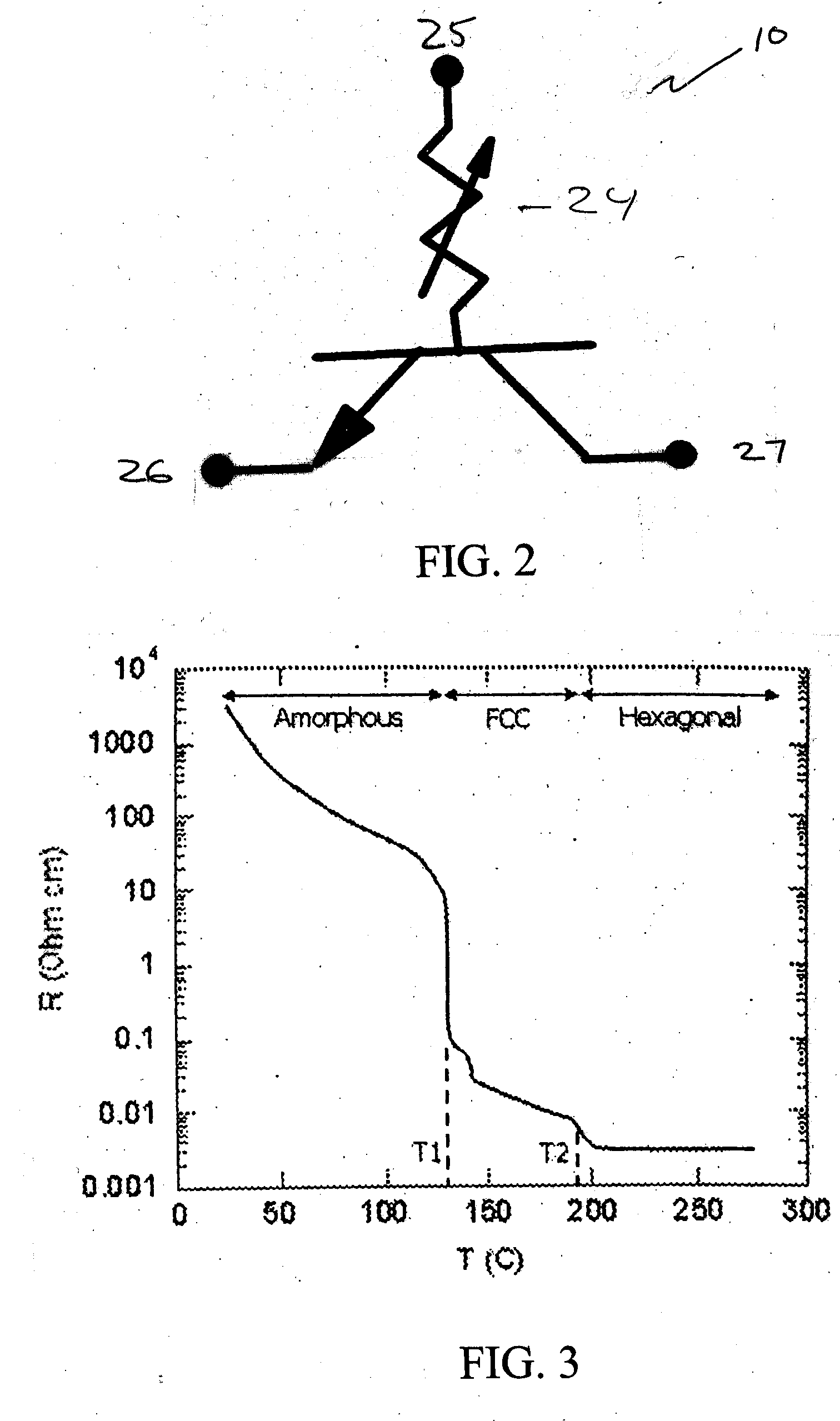
[0042] The present invention provides a memory device comprising a hybrid MOSFET and bipolar transistor, where the crystalline state of a phase change material is controlled by indirect heating. The present invention is now discussed in more detail referring to the drawings that accompany the present application. In the accompanying drawings, like and or corresponding elements are referred to by like reference numbers.

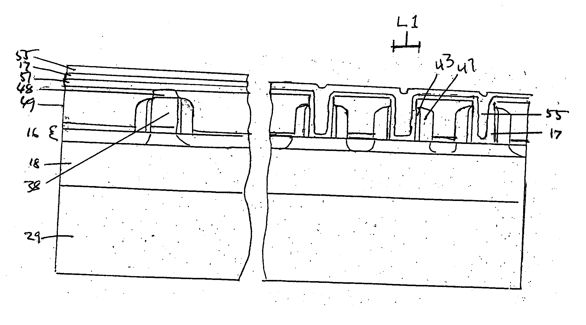
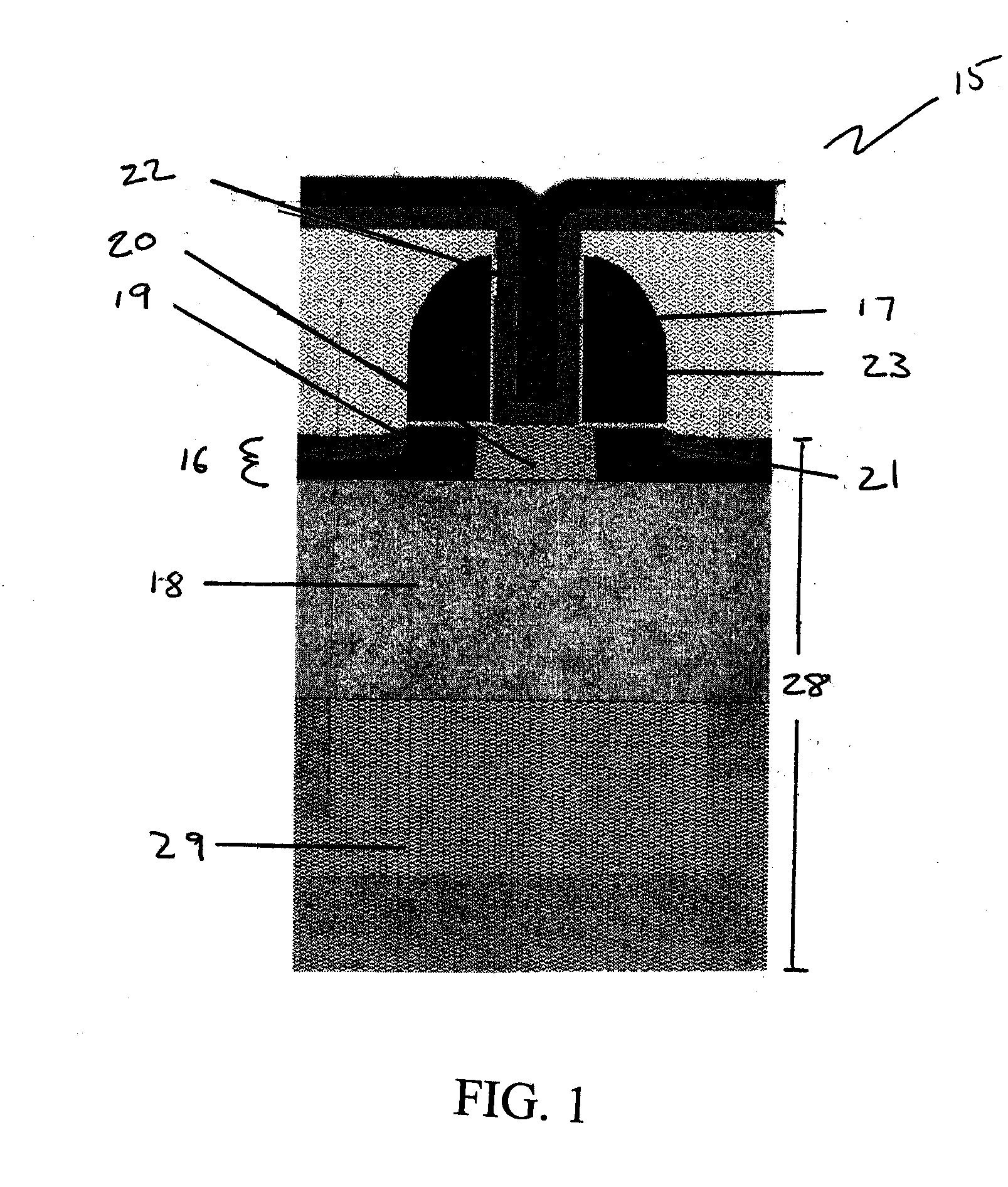
[0043] Reference is first made to FIG. 1, which illustrates a phase change memory device 15 comprising a hybrid metal oxide semiconductor field effect transistor (MOSFET) / bipolar junction transistor having a phase change material 17 that functions as the gate dielectric of a MOSFET or the base contact of a bipolar junction transistor, depending on the crystalline state of the phase change material 17.

[0044] The phase change memory device 15 is formed on a sili-con-on-insulator substrate 28 including a silicon-containing upper layer 16 (hereinafter the SOI layer), ins...


PUM


Abstract

The present invention includes a method for forming a phase change material memory device and the phase change memory device produced therefrom. Specifically, the phase change memory device includes a semiconductor structure including a substrate having a first doped region flanked by a set of second doped regions; a phase change material positioned on the first doped region; and a conductor positioned on the phase change material, wherein when the phase change material is a first phase the semiconductor structure operates as a bipolar junction transistor, and when the phase change material is a second phase the semiconductor structure operates as a field effect transistor.

Description

BACKGROUND OF INVENTION [0001] 1. Field of the Invention [0002] This invention relates to semiconducting devices, and more particularly to a memory device including a phase change material that has electrical properties of a field effect transistor and / or bipolar transistor. [0003] 2. Background of the Invention [0004] Phase change materials may exhibit at least two different states, which may be amorphous or crystalline. The amorphous state involves a more disordered crystal structure. [0005] Transitions between these states may be selectively initiated. The phase change may be induced reversibly. Of particular interest are chalcogenide alloys, which contain one or more elements from Group VI of the Periodic Table of Elements. [0006] Phase change materials are used in standard bulk silicon technologies to form the memory elements of nonvolatile memory devices. Each memory cell may be thought of as a variable resistor, which reversibly changes between higher and lower resistivity st...

Claims


Application Information

Patent Timeline
Patent Type & Authority Applications(United States)
IPC IPC(8): G11C13/00G11C11/56H01L21/06H01L21/331H01L27/10H01L27/105H01L27/12H01L27/24H01L29/00H01L29/68H01L45/00
CPCG11C11/5678H01L29/685H01L27/1203G11C13/0004
Inventor FURKAY, STEPHEN S.HAMANN, HENDRICK T.JOHNSON, JEFFREY B.LAM, CHUNG H.WONG, HON-SUM P.
Owner MARVELL ASIA PTE LTD
Why Eureka
Try Eureka