Photoelectric oscillator

a photoelectric oscillator and oscillator technology, applied in the field of photoelectric oscillators, can solve the problems of difficult improvement of modulation efficiency, unavoidable complex configuration large so as to reduce the size of conventional photoelectric oscillators, shorten the modulator electrodes, and reduce power consumption.

Inactive Publication Date: 2005-09-29
NAT INST OF INFORMATION & COMM TECH
View PDF11 Cites 29 Cited by
  • Summary
  • Abstract
  • Description
  • Claims
  • Application Information

AI Technical Summary

Benefits of technology

[0015] Moreover, provision of a delay circuit capable of delay time adjustment on the optical path between the optical modulator and the photoelectric converter similarly enables regulation of the oscillation frequency and the oscillation mode, making it possible to stabilize radio-frequency oscillation by setting an appropriate delay time.
[0020] The optical modulator can be a reciprocating optical modulator that repeats modulation every reciprocation on a reciprocal optical path. Use of this modulator enables ready generation of radio-order side bands, so that substantially the same effect can be obtained as when modulating with signal whose frequency is a natural number multiple of the modulation signal. The modulation signal is effective when it is in the resonant frequency band of the modulation electrode of the reciprocating optical modulator.
[0021] The optical modulator can instead be a loop optical path optical modulator fabricated by combining an optical modulator having a resonant electrode structure and an optical path of loop structure so as to conduct modulation every circuit of the optical path. Use of such a loop optical path optical modulator enables ready generation of high-order side bands, so that substantially the same effect can be obtained as when modulating with a signal whose frequency is a natural number multiple of the modulation signal. The modulation signal used at this time is effective when it is in the resonant frequency band of the modulation electrode of the loop optical path optical modulator.
[0026] Owing to the use of a resonant electrode structure type optical modulator, the present invention enables size reduction by shortening of the modulator electrode. Moreover, power consumption can be minimized because the improved modulation efficiency lowers the laser beam intensity threshold above which radio-frequency oscillation starts. In addition, the structure of the photoelectric oscillator can be simplified because the filter capability of the modulator makes it possible to impart the feedback circuit with frequency selectivity.
[0027] Owing to the use of an optical modulator having frequency multiplying capability, it is possible to realize photoelectric oscillation operation that exceeds the oscillation frequency limit that can be established using electric circuit technology. That is, notwithstanding that the signal fed back to the modulator is within the band of the electric circuit, a photoelectric oscillator can be realized that in effect achieves high-frequency operation unattainable by the prior art because an optical modulation signal whose frequency is an integral multiple of feedback signal frequency can be produced.

Problems solved by technology

The conventional photoelectric oscillator therefore unavoidably has a complex configuration.
Moreover, the use of a traveling-wave broadband modulator as the optical modulator increases the size of the photoelectric oscillator large and makes improvement of modulation efficiency difficult.
The amount power required during oscillating operation, including that for the laser beam, is therefore disadvantageously large.
This is because, generally, broadband operation of the optical circuit can be adequately achieved but making the electric circuit capable of broadband operation is technically difficult.
Because of the limited bandwidth of the electric circuit, the upper frequency limit of the optical modulated signal obtainable with a conventional photoelectric oscillator is low.

Method used


Image

  • Photoelectric oscillator
  • Photoelectric oscillator
  • Photoelectric oscillator

Examples


Embodiment Construction

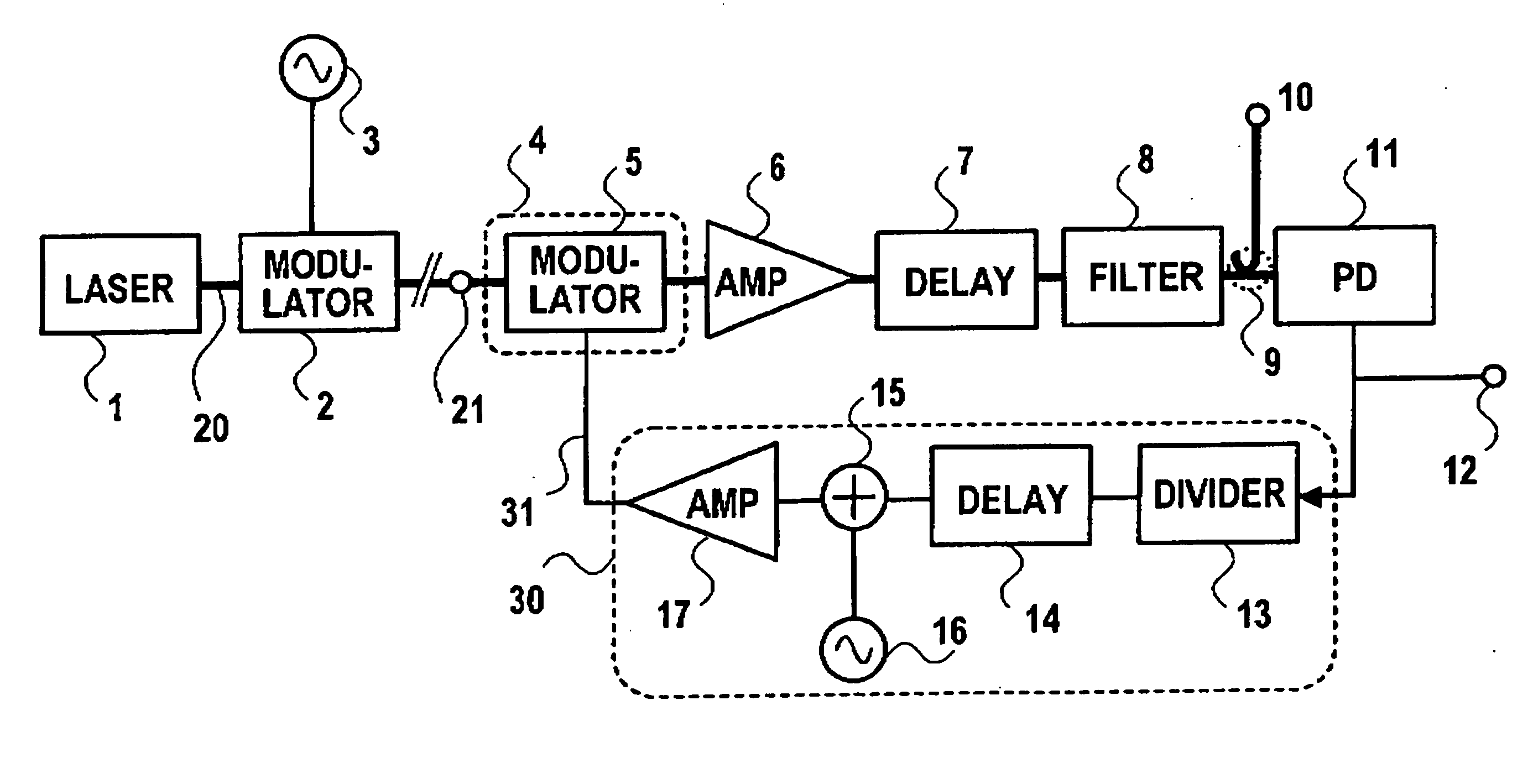
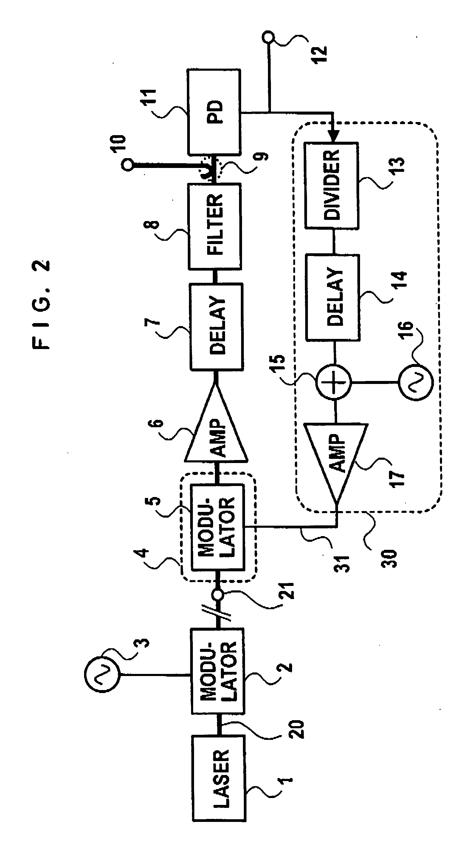
[0078]FIG. 2 is block diagram showing a preferred embodiment of the present invention. A laser beam from a laser beam source 1 is modulated by an optical modulator 2. The modulation signal is supplied from an oscillator 3. This optical modulation is for inducing pull-in phenomenon in the photoelectric oscillator. When the pull-in phenomenon is not utilized, the optical modulator 2 can be omitted. The laser beam is projected from a projection unit 21 and supplied to an optical modulator 5. The optical modulator 5 is a resonant electrode optical modulator or a reciprocating optical modulator. The beam modulated by the optical modulator 5 is amplified by an optical amplifier 6 as required. Amplification is not necessary if the signal intensity is sufficient. After the beam has passed through the optical amplifier 6, it is sent to a delay circuit 7 to be delayed for a prescribed time period. The beam is then passed through an optical filter 8 to extract a signal in the frequency band us...


PUM


Abstract

A photoelectric oscillator includes a laser beam projection unit; an optical modulator on an optical path extending from the projection unit, which optical modulator outputs a modulated signal or an optical signal containing a harmonic of the modulated signal and includes a modulation electrode whose resonant frequency band includes the frequency band of the modulation signal; a photoelectric converter for converting the output of the optical modulator to an electric signal; a feedback circuit for selecting from the radio-frequency electric signal obtained from the photoelectric converter an electric signal to be re-supplied to the optical modulator; and an output section for outputting an optical signal containing the modulation signal or a harmonic of the modulation signal or outputting the modulation signal or a harmonic of the modulation signal. A laser beam of sufficient intensity is input from the projection unit to produce a radio-frequency electric signal in the feedback circuit, and the radio-frequency electric signal or an optical signal containing the radio-frequency electric signal or the radio-frequency signal is output from the photoelectric oscillator.

Description

BACKGROUND OF THE INVENTION [0001] 1. Field of the Invention [0002] This invention relates to a photoelectric oscillator capable of acquiring energy from an incident laser beam and generating a millimeter wave, microwave or other radio-frequency signal, particularly a photoelectric oscillator whose internal optical modulator is provided with a frequency selection characteristic to enable generation of a signal having a high frequency selected by the selection characteristic or a signal having a frequency that is a natural number multiple of the high frequency selected by the selection characteristic. [0003] 2. Description of the Prior Art [0004] The photoelectric oscillator is an oscillator that achieves oscillating operation by feeding back a sideband component produced by laser beam modulation as a modulation signal. The feedback loop of the oscillator is constituted of an optical circuit and an RF (radio-frequency) circuit. During oscillating operation, therefore, it enables, wit...

Claims


Application Information

Patent Timeline
Patent Type & Authority Applications(United States)
IPC IPC(8): H01L27/00
CPCG02F1/2255H04B10/505G02F2203/15G02F2201/58
Inventor KAWANISHI, TETSUYAIZUTSU, MASAYUKISAKAMOTO, TAKAHIDESHINADA, SATOSHI
Owner NAT INST OF INFORMATION & COMM TECH
Why Eureka
Try Eureka