Crystal oscillation circuit

a crystal oscillation circuit and crystal oscillation technology, applied in oscillation generators, pulse techniques, instruments, etc., can solve the problems of increasing the importance and lowering the power consumption of crystal oscillation circuits that are constantly operated in these appliances, so as to achieve stable oscillation, simple and small circuit arrangement, and lower power consumption

Inactive Publication Date: 2006-05-09
CYPRESS SEMICON CORP
View PDF13 Cites 14 Cited by
  • Summary
  • Abstract
  • Description
  • Claims
  • Application Information

AI Technical Summary

Benefits of technology

[0028]The present invention is made in consideration of the foregoing respects, and it is an object of the present invention to provide a crystal oscillation circuit which has a simple and small circuit arrangement and offers stable oscillation at lower power consumption.

Problems solved by technology

Hence, the lower power consumption of the crystal oscillation circuit that is being constantly operated in such an appliance has been an important technical issue.
As described above, the supply of constant current to the oscillating inverter has led to lowering the power consumption of the crystal oscillation circuit.
Hence, the lower power consumption of the crystal oscillation circuit that is constantly operated in these appliances becomes a more and more important technical issue.
However, in the case of using the two-stage operational amplifier as shown in FIG. 11 as the voltage follower, it is necessary to design a frequency characteristic of a negative feedback loop so as not to make the operation of the voltage follower unstable due to its oscillation.
In general, this type of capacitor needs a disadvantageously large capacitance and circuit area.
However, in a case that the load capacitance is small or no stabilization capacitance is specially provided for the constant voltage Vreg, the provision of the phase compensation capacitor may be unnecessary.
This results in increasing the power consumption of the crystal oscillation circuit.
Further, in the method of supplying constant current to the oscillating inverter for reducing the circuit power, in the circuit shown in FIG. 12, since the current defined in the depletion NMOS transistor M114 is supplied to the transistors M110 and M111, the current to be supplied is likely to be adversely influenced by the manufacturing variation of the transistor M114 and thus is not stable.
Hence, if the circuit is designed so that the oscillation may be kept even at a lower voltage of the power supply Vdd, the current is made larger than required if the voltage of the power supply Vdd is high and moreover the current is likely to be adversely influenced by the manufacturing variation of the transistor M115.
This was a problem as well.
These two circuits disadvantageously make the overall oscillation circuit complicated.

Method used


Image

  • Crystal oscillation circuit
  • Crystal oscillation circuit
  • Crystal oscillation circuit

Examples


first embodiment

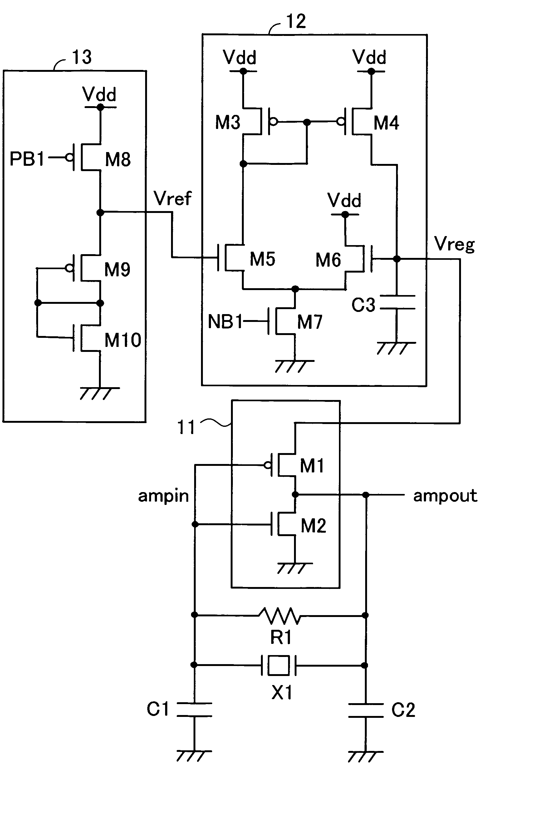
[0045]Hereafter, the embodiments of the present invention will be described with reference to the accompanying drawings. FIG. 1 shows a crystal oscillation circuit according to the present invention. As shown, the crystal oscillation circuit is arranged to have an oscillating amplifier 11, a constant voltage generator 12, a replica circuit 13, a resistor R1, capacitors C1 and C2, and a crystal oscillator X1. The oscillating amplifier 11 is composed of transistors Ml and M2. The constant voltage generator 12 is composed of PMOS transistors M3 and M4, NMOS transistors M5 to M7 and a capacitor C3. The replica circuit 13 is composed of PMOS transistors M8 and M9 and an NMOS transistor M10.

[0046]The transistors M1 and M2 composing the oscillating amplifier 11 operate to excite the resonator (positive feedback circuit) composed of the capacitors C1 and C2 and a crystal oscillator X1. The resistor R1 is a feedback resistor for specifying the operating points of the transistors M1 and M2.

[0...

second embodiment

[0080]As described above, the voltage follower composed of a one-stage amplifier allows a maximum current to be easily designed. This makes it possible to realize the characteristic in which the power is not greatly increased if the actual consumed current is somewhat shifted from the designed value. Through the use of this characteristic, by adding the resistor R3 to the replica circuit, the crystal oscillation circuit enables to reduce the current flowing through the replica circuit.

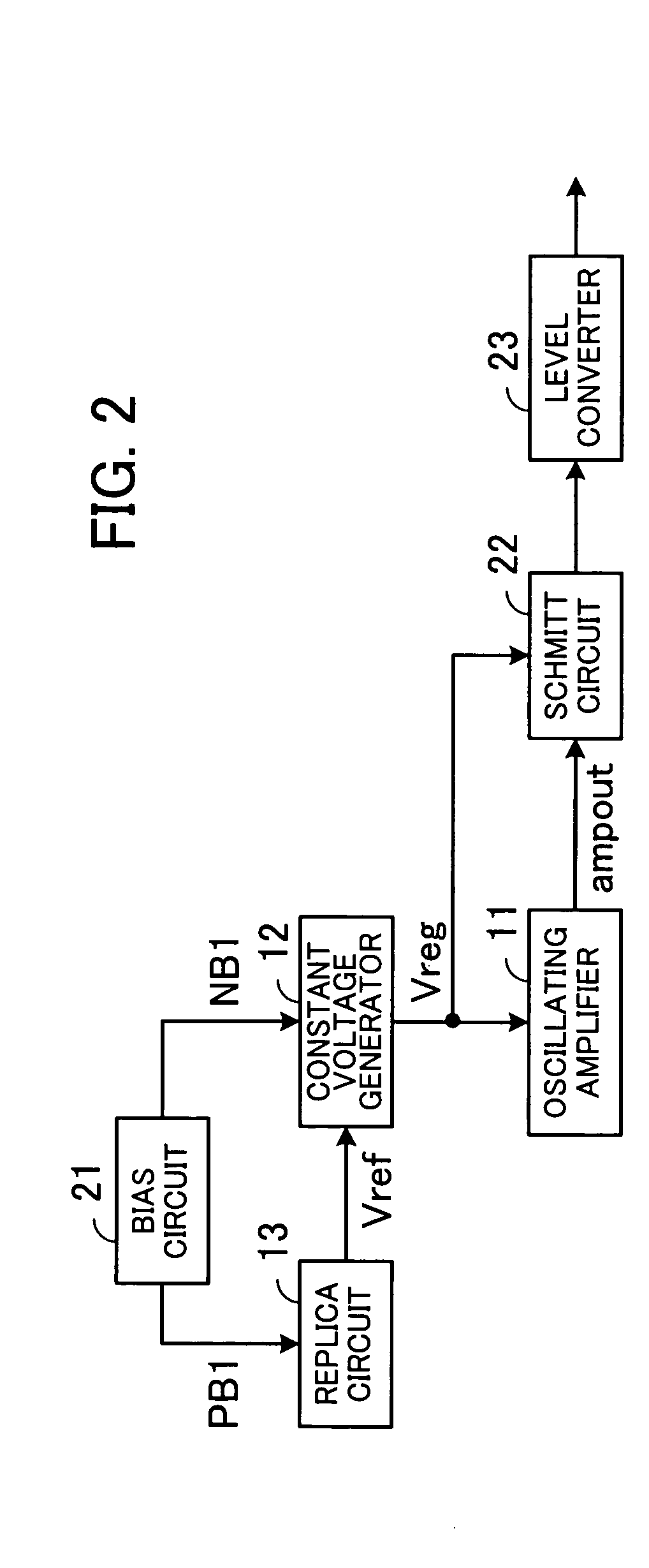
[0081]Like the crystal oscillation circuit according to the first embodiment, the crystal oscillation circuit according to the second embodiment may be used in combination with the bias circuit 21, the Schmitt circuit 22, and the level converter 23.

third embodiment

[0082]In turn, the description will be oriented to the crystal oscillation circuit according to the present invention. FIG. 6 shows this crystal oscillating circuit. In the crystal oscillation circuit, the drain of the transistor M6 included in the circuit shown in FIG. 5 is inputted with not the voltage from the power supply Vdd but the constant voltage Vreg. In FIG. 6, the same components as those shown in FIG. 5 have the same reference numbers and are not described herein.

[0083]As shown in FIG. 6, the drain of the NMOS transistor M30 is connected with the drain of the transistor M4. The source of the transistor M30 is connected with the source of the transistor M5 and the drain of the transistor M7. The gate of the transistor M30 is connected with the drain of the transistor M4, the capacitor C3 and the drain of the transistor M28.

[0084]Also, the crystal oscillation circuit shown in FIG. 6 is different from the circuit shown in FIG. 5 in a respect that the constant voltage Vreg i...


PUM


Abstract

A crystal oscillation circuit has a reduced circuit area and enables to stably oscillate at low consumed current. The crystal oscillation circuit includes an oscillating amplifier and a constant voltage generator. The oscillating amplifier excites a resonator composed of a resistor, a crystal oscillator and a capacitor. The constant voltage generator includes a one-stage differential circuit composed of a transistor and a capacitor for suppressing transient fluctuation of a constant voltage Vreg for generating the constant voltage Vreg served as a supply voltage for the oscillating amplifier. By generating the constant voltage Vreg through the one-stage differential circuit, the phase lag of the constant voltage Vreg reaches 90 degrees at most. This eliminates the necessity of a phase compensation capacitor, resulting in making the circuit area smaller and realizing the stable oscillation at low consumed current.

Description

[0001]This application is a continuing application, filed under 35 U.S.C. §111(a), of International Application PCT / JP2003 / 004794, filed Apr. 15, 2003.BACKGROUND OF THE INVENTION[0002](1) Field of the Invention[0003]The present invention relates to a crystal oscillation circuit, and more particularly to a crystal oscillation circuit which is served to oscillate on the basis of an oscillation frequency of a crystal oscillator.[0004](2) Description of the Related Art[0005]An oscillation circuit provided with a crystal oscillator is widely used in various appliances such as a watch, a cellular phone and a computer terminal because the oscillation circuit is stable in frequency. For these portable electronic appliances., the life of a cell built therein is a significant performance characteristic. Hence, the lower power consumption of the crystal oscillation circuit that is being constantly operated in such an appliance has been an important technical issue.[0006]In order to lower the p...

Claims


Application Information

Patent Timeline
Patent Type & Authority Patents(United States)
IPC IPC(8): H03B5/36H03L1/00H03L1/02
CPCH03B5/364
Inventor TACHIBANA, SUGURUMORISHITA, TOMONARIKIHARA, FUKUJIKUBOTA, MAKOTO
Owner CYPRESS SEMICON CORP
Why Eureka
Try Eureka