Amplifying solid-state imaging device

a solid-state imaging and amplifier technology, applied in the direction of color television details, television systems, radio control devices, etc., can solve the problem of reducing the charge voltage conversion rate , achieve the effect of reducing the pixel size and high-quality images

Inactive Publication Date: 2005-09-29
SHARP KK
View PDF13 Cites 26 Cited by
  • Summary
  • Abstract
  • Description
  • Claims
  • Application Information

AI Technical Summary

Benefits of technology

[0015] The present invention is to solve the problem and has an object to provide an amplifying solid-state imaging device capable of obtaining a high-quality image and reducing the pixel size.

Problems solved by technology

However, if three to four MOS transistors are necessary per pixel, then the arrangement becomes a limitation on reducing the pixel size, and therefore, a method for reducing the transistor count per pixel is proposed (refer to, for example, JP 09-46596 A).
However, the conventional amplifying solid-state imaging device causes the following problems in terms of the construction and operation.
Accordingly, there is a problem that the charge voltage conversion rate η is reduced as number of photodiodes and the transfer transistors connected to the common signal charge storage section increases.

Method used


Image

  • Amplifying solid-state imaging device
  • Amplifying solid-state imaging device
  • Amplifying solid-state imaging device

Examples


first embodiment

The First Embodiment

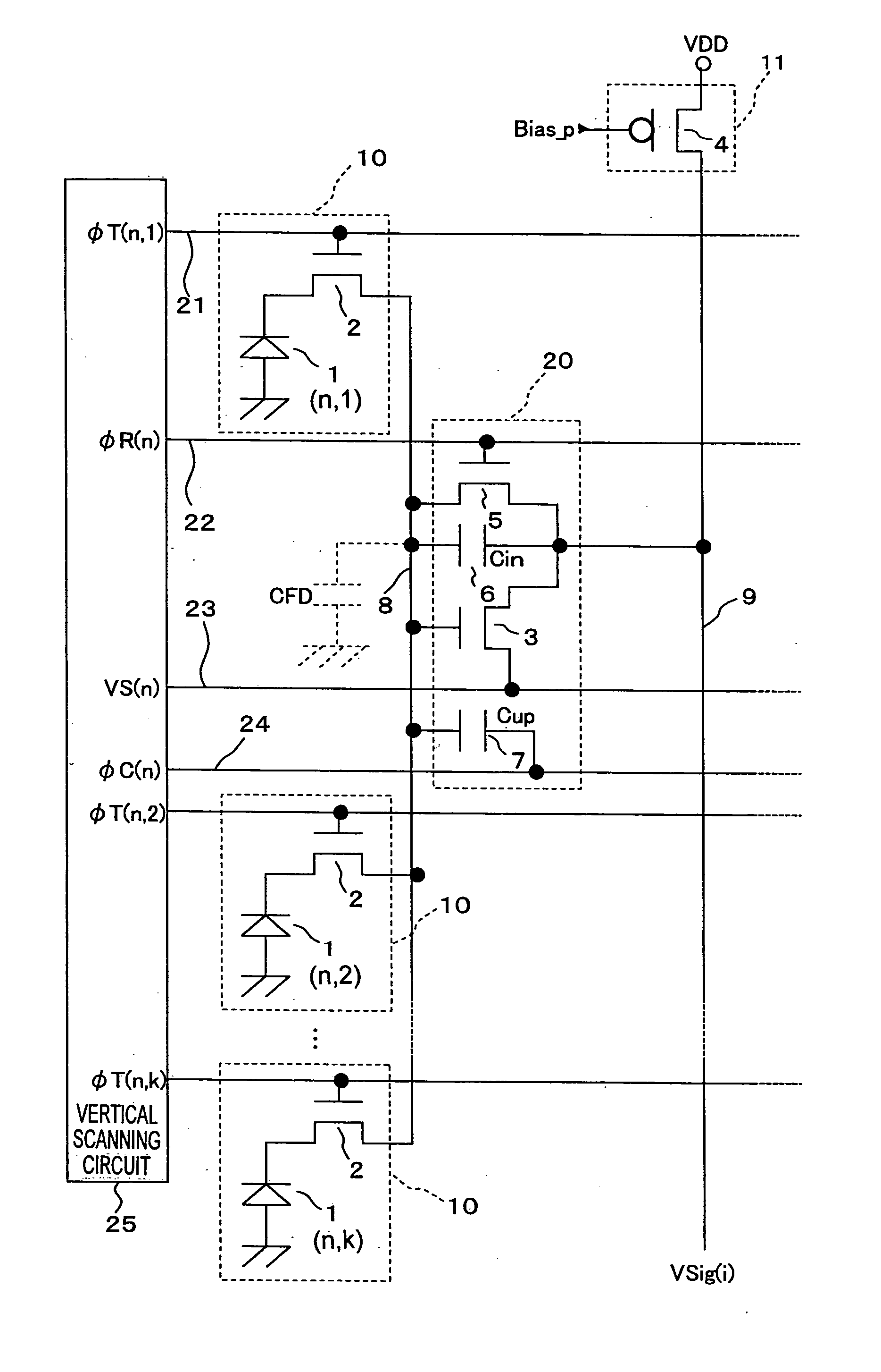
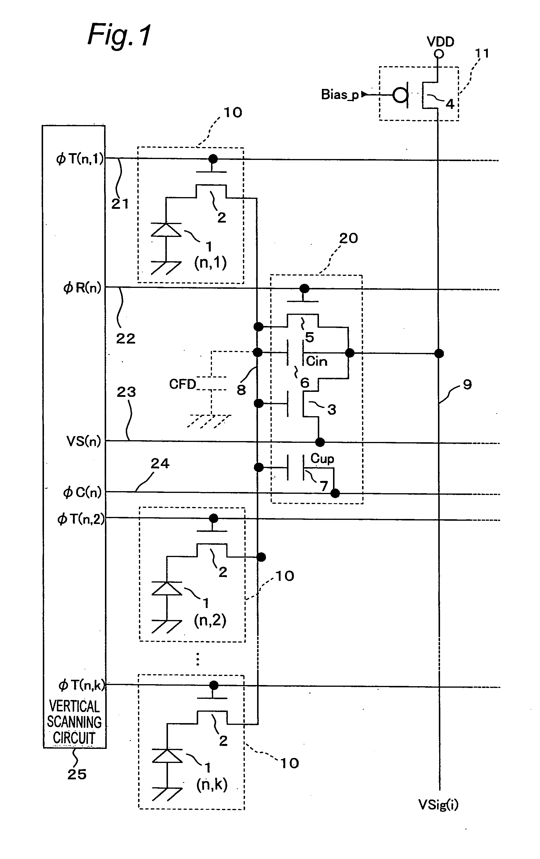
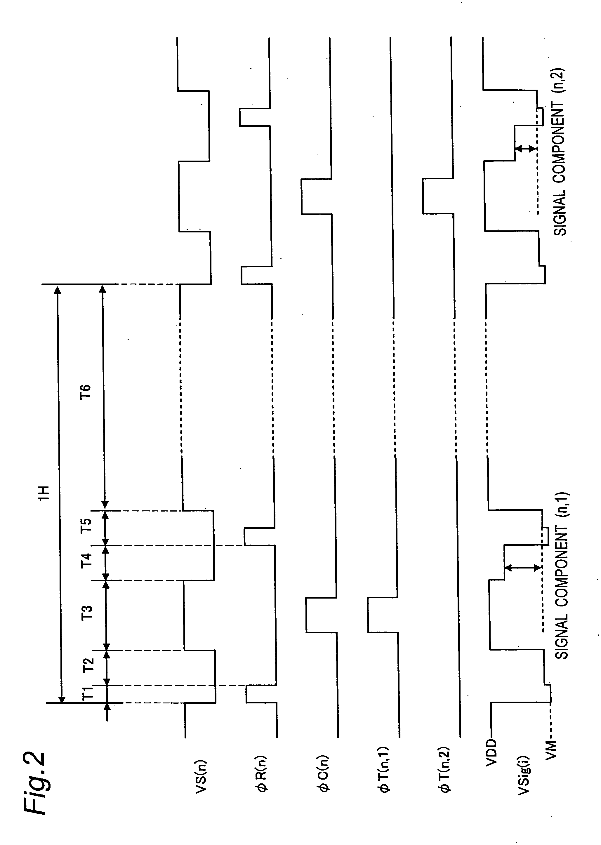
[0102]FIG. 1 is a circuit diagram showing the construction of a two-dimensional amplifying solid-state imaging device as one example of an amplifying solid-state imaging device of the first embodiment of the present invention. In the two-dimensional amplifying solid-state imaging device, a plurality of pixels are two-dimensionally arranged in a matrix form.

[0103] The figure shows a photoelectric conversion transfer section 10 existing in every pixel, a switched capacitor amplifier section 20 shared by k photoelectric conversion transfer sections 10 in the vertical direction, a power supply side load 11 exemplified by a constant current load transistor 4 shared by all the switched capacitor amplifier sections 20 existing in a column i, and a vertical scanning circuit 25 as one example of a control section. In FIG. 1, only the i-th column of the photoelectric conversion transfer sections 10 of a plurality of rows and a plurality of columns are shown, and the switc...

second embodiment

The Second Embodiment

[0132]FIG. 6 is a circuit diagram showing the construction of a two-dimensional amplifying solid-state imaging device as one example of an amplifying solid-state imaging device of the second embodiment of the present invention. The two-dimensional amplifying solid-state imaging device of the second embodiment has the same construction as that of the first embodiment except for the connection of the reset transistor, and the same constituents are denoted by the same reference numerals with no description provided therefor. A difference to the two-dimensional amplifying solid-state imaging device of the first embodiment is as follows. In contrast to the first embodiment in which the reset transistor 5 is inserted between the input and output of the amplification transistor 3, a reset transistor 5 in the second embodiment is inserted between an input portion of an amplification transistor 3 and a light shielding pattern 26 as one example of a potential portion to w...

third embodiment

The Third Embodiment

[0143]FIG. 9 is a circuit diagram showing the construction of a two-dimensional amplifying solid-state imaging device as one example of an amplifying solid-state imaging device of the third embodiment of the present invention. The two-dimensional amplifying solid-state imaging device of the third embodiment has the same construction as that of the first embodiment except for the connection of the reset transistor, and the same constituents are denoted by the same reference numerals with no description provided therefor. A difference to the amplifying solid-state imaging device of the first embodiment is as follows. In contrast to the first embodiment in which the reset transistor 5 is inserted between the input and output of the amplification transistor 3, the reset transistor 5 is inserted between the input side of the amplification transistor 3 and a potential control line 24 to which the control pulse φC(n) is applied in the third embodiment. The source of the...


PUM


Abstract

An input side of a switched capacitor amplifier section is connected to output sides of transfer transistors of a photoelectric conversion transfer section group comprised of a prescribed number of a plurality of photoelectric conversion transfer sections, each of which has a photodiode and a transfer transistor. An output side of the switched capacitor amplifier section is connected to a vertical signal line. The switched capacitor amplifier section has a signal charge storage section, an amplification transistor whose an input side is connected to the signal charge storage section, a capacitor connected between input and output sides of the amplification transistor and a reset transistor. A voltage at the ground terminal of an inverting amplifier, which is constructed of a constant current load transistor connected to the output side of the amplification transistor via the vertical signal line and the amplification transistor, is controlled by a vertical scanning circuit.

Description

[0001] This nonprovisional application claims priority under 35 U.S.C. §119(a) on Patent Application No. 2004-091544 filed in Japan on Mar. 26, 2004, the entire contents of which are hereby incorporated by reference.BACKGROUND OF THE INVENTION [0002] The present invention relates to amplifying solid-state imaging devices and to a technique for achieving a low-noise amplifying solid-state imaging device with small-sized pixels. [0003] Conventionally, an amplifying solid-state imaging device, which has a pixel section provided with an amplification function and a scanning circuit provided at the periphery of the pixel section and reads image data by means of the scanning circuit, has been proposed as an amplifying solid-state imaging device. In particular, an APS (Active Pixel Sensor) type image sensor having a CMOS (Complementary Metal Oxide Semiconductor) structure advantageous in integrating the pixel construction with a peripheral driving circuit and a signal processing circuit is...

Claims


Application Information

Patent Timeline
Patent Type & Authority Applications(United States)
IPC IPC(8): H04N5/335H04N5/374H01L27/146
CPCH04N5/37457H04N25/59H04N25/778H04N25/76H04N25/75
Inventor KOYAMA, EIJI
Owner SHARP KK
Why Eureka
Try Eureka