Circuit for controlling an enabling time of an internal control signal according to an operating frequency of a memory device and the method thereof
- Summary
- Abstract
- Description
- Claims
- Application Information
AI Technical Summary
Benefits of technology
Problems solved by technology
Method used
Image
Examples
Embodiment Construction
[0042] Reference will now be made in greater detail to a preferred embodiment of the invention, an example of which is illustrated in the accompanying drawings. Wherever possible, the same reference numerals will be used throughout the drawings and the description to refer to the same or like parts.
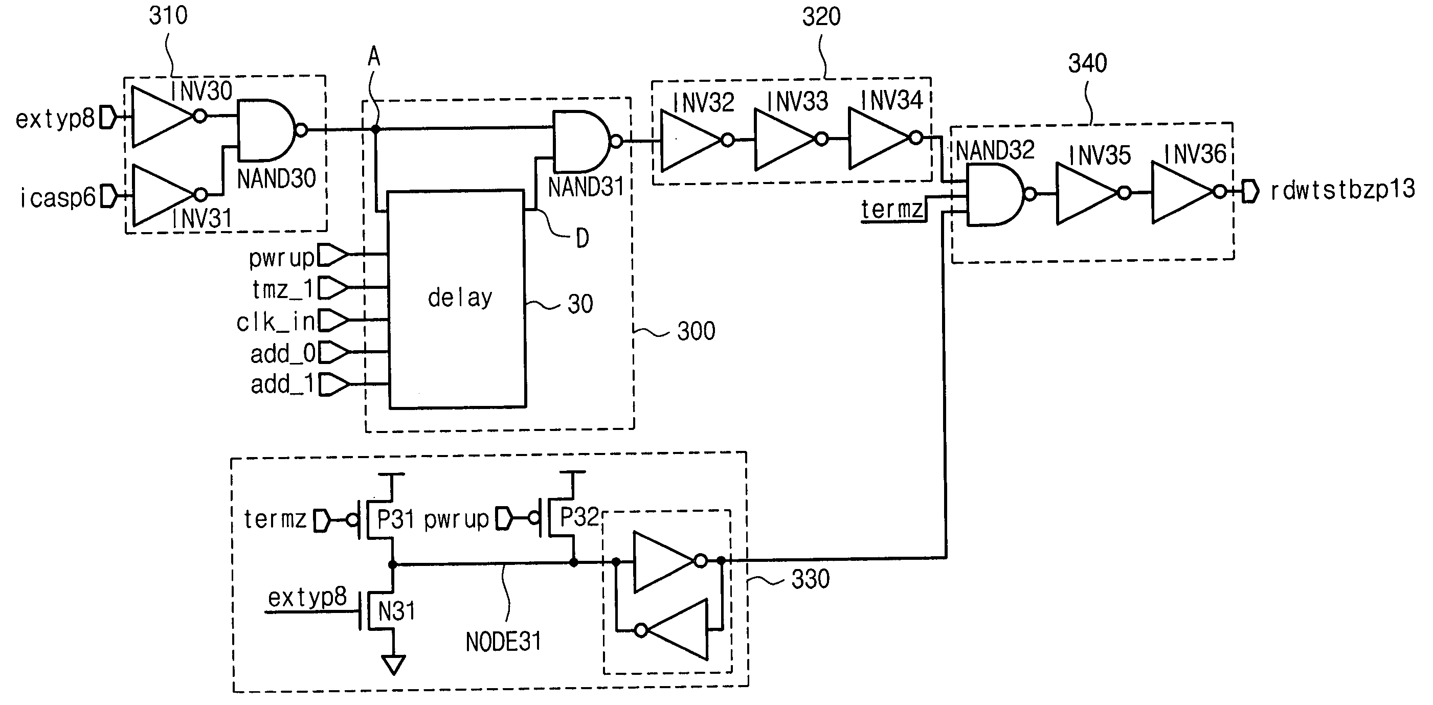
[0043]FIG. 3 illustrates an exemplary embodiment of a read / write strobe pulse generator in accordance with the present invention.
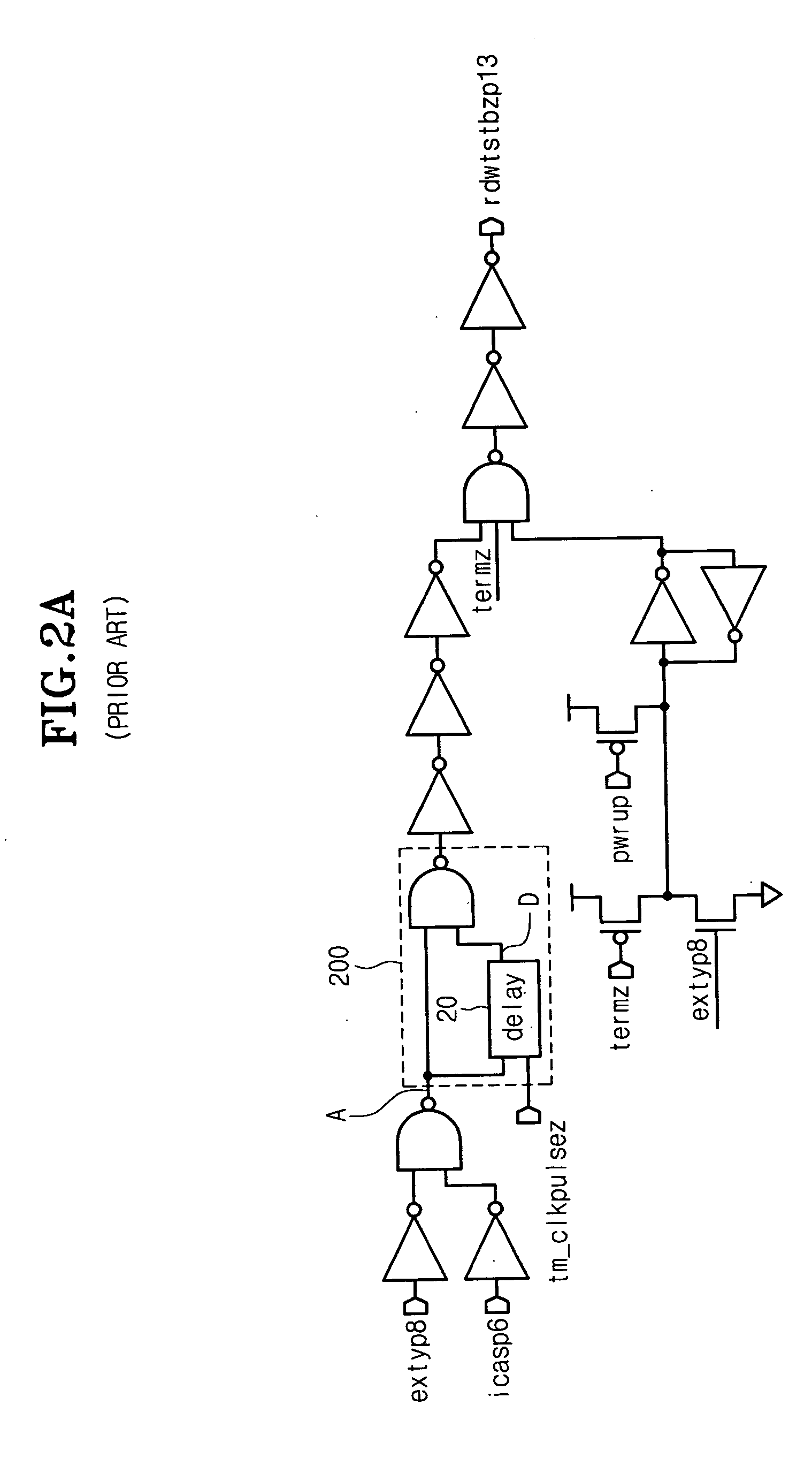
[0044] The circuit of FIG. 3 is different from the circuit of FIG. 2A in that a delay circuit 30 in a pulse width adjusting circuit 300 is controlled by a clock signal clk_in and address signals add_0 and add_1.
[0045] The circuit of FIG. 3 is comprised of an input signal receiver 310, a pulse width adjusting circuit 300, a signal transmission circuit 320, a test mode circuit 330, and an output circuit 340.
[0046] The input signal receiver 310 includes inverters INV30 and INV31, and a NAND gate NAND30. An input signal extyp8 is applied to the inverter INV30 an...
PUM
 Abstract
Description
Claims
Application Information


