

Semiconductor circuit apparatus with power save mode
a technology of circuit apparatus and power saving mode, which is applied in the direction of waveguide type devices, pulse techniques, instruments, etc., can solve the problems of increasing power consumption, long time to go into the active mode from the standby mode, and complicated circuit configuration and sequence for mode switching, so as to achieve speed return and power consumption reduction
- Summary
- Abstract
- Description
- Claims
- Application Information
AI Technical Summary
Benefits of technology
Problems solved by technology
Method used
Image

Examples
embodiment 1
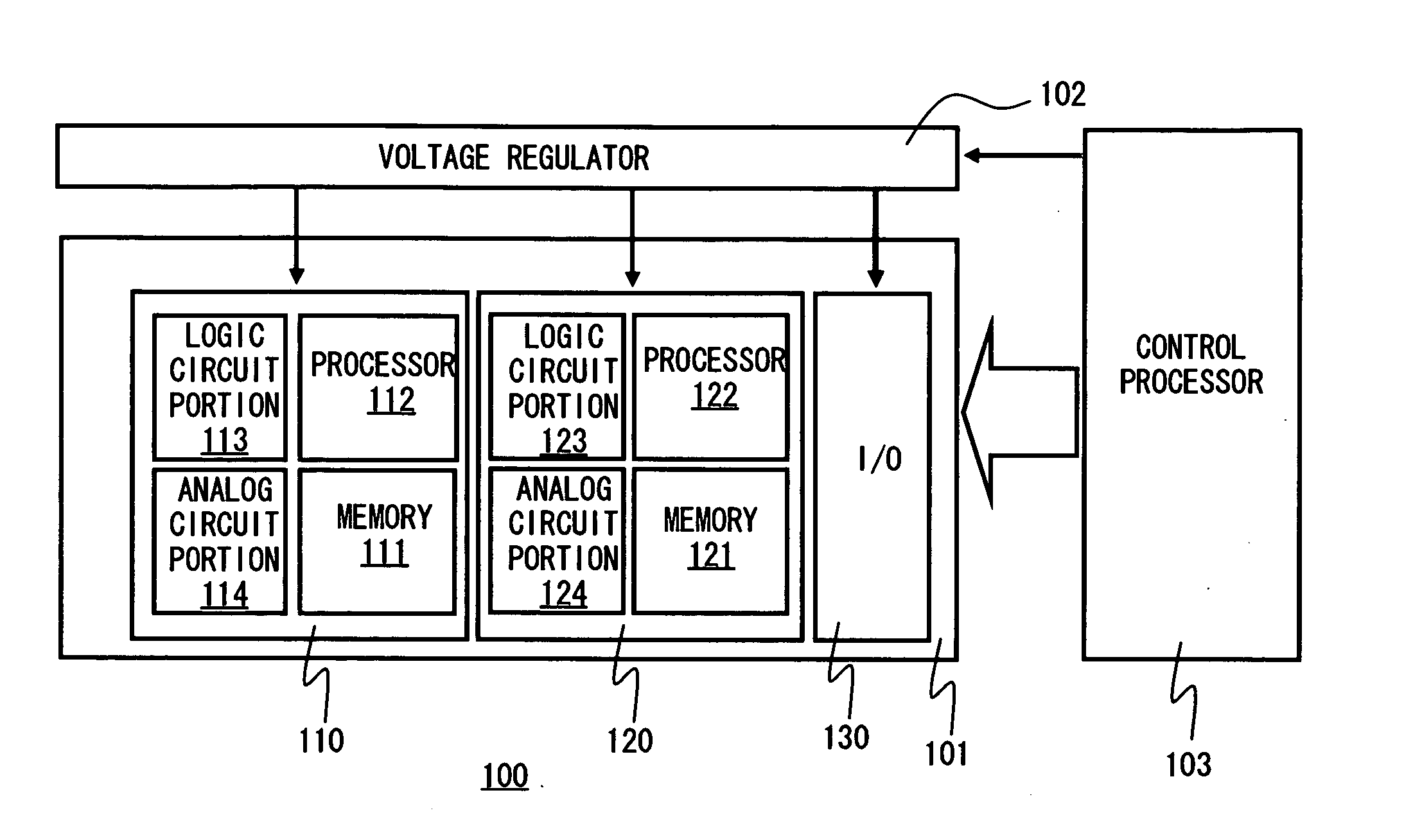
[0027]FIG. 1 is a schematic diagram illustrating a semiconductor circuit apparatus 100 according to this embodiment. Referring to FIG. 1, a voltage regulator 102 provides a semiconductor circuit chip 101 with power supply voltages, including a higher voltage Vdd and lower voltage Vss. A control processor 103 controls the semiconductor circuit chip 101 and the voltage regulator 102. In this embodiment, the voltage regulator 102 and control processor 103 are formed outside of the semiconductor circuit chip 101, namely formed in a different chip than the semiconductor circuit chip 101.
[0028] The semiconductor circuit chip 101 comprises a first circuit block 110, second circuit block 120, and I / O circuit 130 which is a interface circuit performs date input / output with external circuits. The firs and the second circuit blocks communicate data with external circuits through the I / O circuit 130. Furthermore, the first circuit block 110 comprises a memory 111, processor 112, a logic circui...
embodiment 2
[0041] In mode switching, it is important to reduce leakage current during the standby mode to reduce the power consumption, as well as high speed switching. Sub-threshold leakage current and gate leakage current are known as the leak current. A MOS transistor with low threshold voltage can not turns off completely, leading to a large amount of sub-threshold leakage current. In a MOS transistor with a thin gate oxide film, tunnel leakage current flows through the thin gate oxide film. The tunnel leakage current flows from a gate to source / drain of from the source / drain to the gate.
[0042] Proper design for gate oxide film thickness is important to allow high speed operation and reduce leakage current. A thinner gate oxide film improves the operation performance, but it increases leakage current. On the other hand, thicker gate oxide film reduces leakage current, but it lowers the operation performance. Therefore, relatively thin gate oxide films are used in a circuit block which is ...
embodiment 3
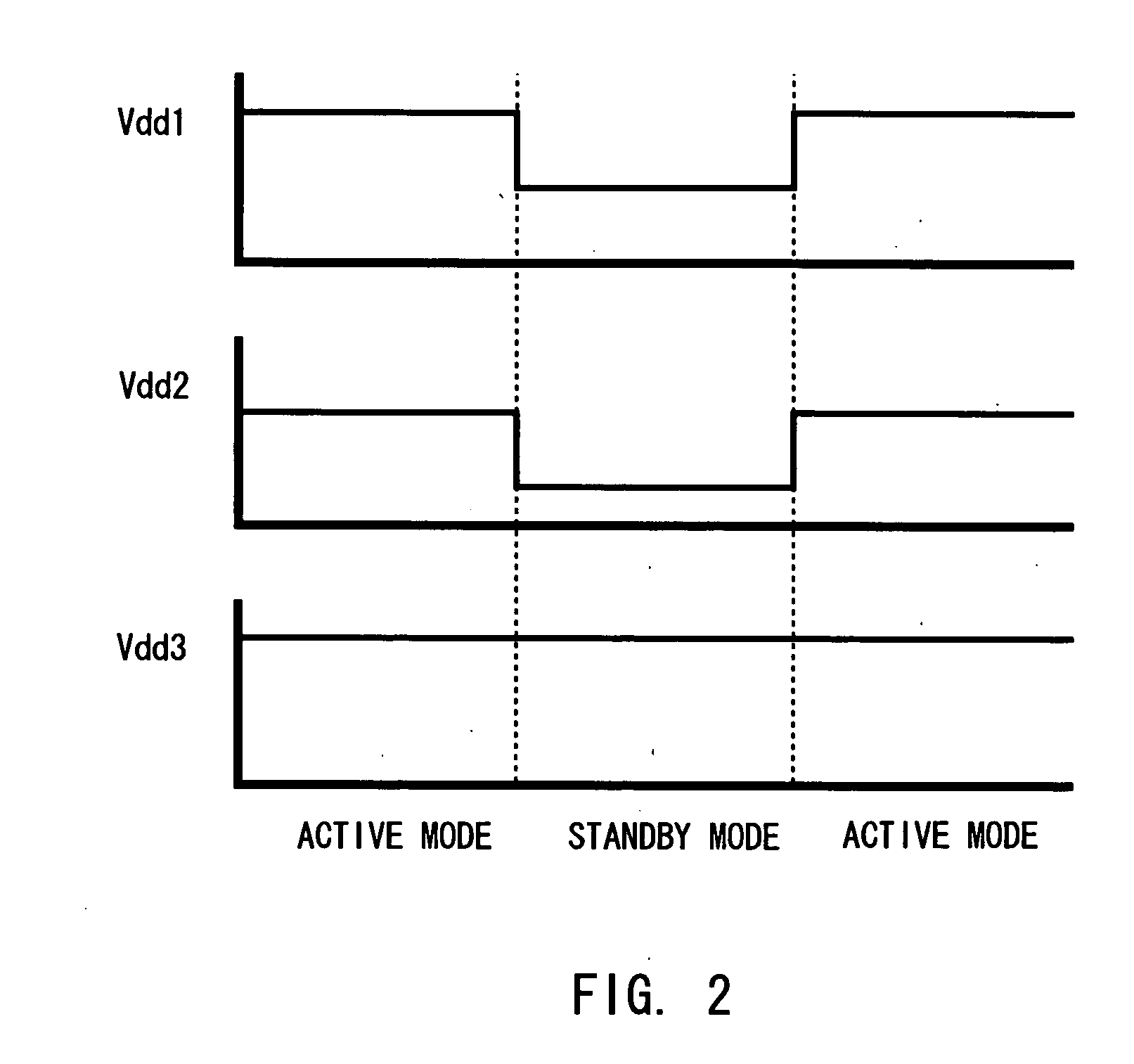
[0047] It is preferable to control a substrate potential to decrease leakage current during the standby mode. FIG. 5 is a schematic diagram illustrating a semiconductor circuit apparatus according to the present embodiment. A substrate bias circuit 501 provides a substrate bias potential. The substrate bias circuit 501 is formed outside the semiconductor circuit chip 101, and it is formed on the same chip as the voltage regulator 102 in FIG. 5. Other configuration is substantially the same as FIG. 1 and details are omitted.
[0048] In a P type substrate, for example, the substrate potential during operation is generally set to ground. Reduction of the substrate potential (deviation in a negative direction) results in an increase in the threshold voltages of transistors. On the other hand, increase of the substrate potential (deviation in a positive direction) results in a decrease in the threshold voltages of transistors. An increase in the threshold voltage of a transistor results i...
PUM
 Abstract
Description
Claims
Application Information